Thermal properties in mesoscopics: physics and ... - ResearchGate
Thermal properties in mesoscopics: physics and ... - ResearchGate
Thermal properties in mesoscopics: physics and ... - ResearchGate

Create successful ePaper yourself
Turn your PDF publications into a flip-book with our unique Google optimized e-Paper software.
<strong>Thermal</strong> <strong>properties</strong> <strong>in</strong> <strong>mesoscopics</strong>: <strong>physics</strong> <strong>and</strong> applications from<br />
thermometry to refrigeration<br />
Contents<br />
Francesco Giazotto, 1, 2, ∗ Tero T. Heikkilä, 1, 3, † Arttu Luukanen, 4 Alex<strong>and</strong>er M. Sav<strong>in</strong>, 1 <strong>and</strong> Jukka P. Pekola 1<br />
1 Low Temperature Laboratory, Hels<strong>in</strong>ki University of Technology, P.O. Box 2200, FIN-02015 HUT, F<strong>in</strong>l<strong>and</strong><br />
2 NEST-INFM <strong>and</strong> Scuola Normale Superiore, I-56126 Pisa, Italy<br />
3 Department of Physics <strong>and</strong> Astronomy, University of Basel, Kl<strong>in</strong>gelbergstr. 82, CH-4056 Basel, Switzerl<strong>and</strong><br />
4 National Institute of St<strong>and</strong>ards <strong>and</strong> Technology, Quantum Electrical Metrology Division, 325 Broadway, Boulder CO<br />
80305 USA ‡<br />
(Dated: December 2, 2005)<br />
We present an overview of the thermal <strong>properties</strong> of mesoscopic structures. The discussion <strong>in</strong> this<br />
Review is based on the concept of electron energy distribution, <strong>and</strong> <strong>in</strong> particular, on controll<strong>in</strong>g <strong>and</strong><br />
prob<strong>in</strong>g it. The temperature of the electron gas is determ<strong>in</strong>ed by this distribution: refrigeration<br />
is equivalent to narrow<strong>in</strong>g it, <strong>and</strong> thermometry is prob<strong>in</strong>g its convolution with a function characteriz<strong>in</strong>g<br />
the measur<strong>in</strong>g device. Temperature exists, strictly speak<strong>in</strong>g, only <strong>in</strong> quasi-equilibrium,<br />
where the distribution is the Fermi-Dirac one. Interest<strong>in</strong>g non-equilibrium deviations can also occur,<br />
due to slow relaxation rates of the electrons, e.g., among themselves or with lattice phonons.<br />
Observation <strong>and</strong> applications of non-equilibrium phenomena are also discussed. Our focus is at<br />
low temperatures, primarily below 4 K, where physical phenomena on mesoscopic scales <strong>and</strong> hybrid<br />
comb<strong>in</strong>ations of various types of materials, e.g., of superconductors, normal metals, <strong>in</strong>sulators<br />
<strong>and</strong> doped semiconductors, open up a rich variety of device concepts. The present Review starts<br />
with the <strong>in</strong>troduction to the theoretical concepts <strong>and</strong> results on thermal <strong>properties</strong> of mesoscopic<br />
structures. We then focus on thermometry <strong>and</strong> refrigeration with emphasis on the experimental<br />
status. An immediate application field of solid-state refrigeration <strong>and</strong> thermometry is <strong>in</strong> ultrasensitive<br />
radiation detection, which we discuss <strong>in</strong> depth. The Review also gives a summary of<br />
pert<strong>in</strong>ent fabrication methods of the presented devices.<br />
I. Introduction 2<br />
II. <strong>Thermal</strong> <strong>properties</strong> of mesoscopic scale hybrid<br />
structures at sub-kelv<strong>in</strong> temperatures 2<br />
A. Boltzmann equation <strong>in</strong> a diffusive wire 3<br />
B. Boundary conditions 4<br />
C. Collision <strong>in</strong>tegrals for <strong>in</strong>elastic scatter<strong>in</strong>g 5<br />
1. Electron-electron scatter<strong>in</strong>g 5<br />
2. Electron–phonon scatter<strong>in</strong>g 6<br />
D. Quasiequilibrium limit 7<br />
E. Observables 8<br />
1. Currents 8<br />
2. Noise 9<br />
F. Examples on different systems 10<br />
1. Normal-metal wire between normal-metal<br />
reservoirs 10<br />
2. Superconduct<strong>in</strong>g tunnel structures 11<br />
3. Superconductor-normal-metal structures with<br />
transparent contacts 12<br />
G. Heat transport by phonons 15<br />
H. Heat transport <strong>in</strong> a metallic reservoir 16<br />
III. Thermometry on mesoscopic scale 17<br />
A. Hybrid junctions 18<br />
1. NIS thermometer 18<br />
2. SIS thermometer 19<br />
3. Proximity effect thermometry 19<br />
B. Coulomb blockade thermometer, CBT 20<br />
∗ Electronic address: F.Giazotto@sns.it<br />
† Electronic address: Tero.T.Heikkila@hut.fi<br />
‡ Present address: MilliLab, VTT Information Technology, P.O.<br />
Box 1202, FIN-02044 VTT, F<strong>in</strong>l<strong>and</strong><br />
C. Shot noise thermometer, SNT 22<br />
D. Thermometry based on the temperature dependent<br />
conductance of planar tunnel junctions 23<br />
E. Anderson-<strong>in</strong>sulator th<strong>in</strong> film thermometry 23<br />
IV. <strong>Thermal</strong> detectors <strong>and</strong> their characteristics 24<br />
A. Effect of operat<strong>in</strong>g temperature on the performance of<br />
thermal detectors 24<br />
B. Bolometers: Cont<strong>in</strong>uous excitation 25<br />
1. Hot electron bolometers 27<br />
2. Hot phonon bolometers 28<br />
C. Calorimeters: Pulsed excitation 30<br />
D. Future directions 31<br />
V. Electronic refrigeration 31<br />
A. General pr<strong>in</strong>ciples 32<br />
B. Peltier refrigerators 32<br />
C. Superconduct<strong>in</strong>g electron refrigerators 33<br />
1. (SI)NIS structures 33<br />
2. S1IS2(IS1) structures 37<br />
3. SSmS structures 38<br />
4. SF systems 39<br />
5. HTc NIS systems 40<br />
6. Application of (SI)NIS structures to lattice<br />
refrigeration 40<br />
7. Josephson transistors 42<br />
D. Perspective types of refrigerators 43<br />
1. Thermionic refrigerators 44<br />
2. Application of low-dimensional systems to<br />
electronic refrigeration 44<br />
VI. Device fabrication 45<br />
A. Structure typologies <strong>and</strong> material considerations 45<br />
B. Semiconductor growth techniques 46<br />
C. Th<strong>in</strong>-film metals deposition methods 46<br />
1. <strong>Thermal</strong> evaporation 46<br />
2. Sputter deposition 47<br />
D. Th<strong>in</strong> film <strong>in</strong>sulators 47
E. Lithography <strong>and</strong> etch<strong>in</strong>g techniques 48<br />
F. Tunnel barriers 49<br />
1. Oxide barriers 49<br />
2. Schottky barriers 49<br />
VII. Future prospects 50<br />
Acknowledgments 50<br />
References 51<br />
I. INTRODUCTION<br />
Solid state mesoscopic electronic systems provide a<br />
micro-laboratory to realize experiments on low temperature<br />
<strong>physics</strong>, to study quantum phenomena such<br />
as fundamental relaxation mechanisms <strong>in</strong> solids, <strong>and</strong> a<br />
way to create advanced cryogenic devices. In a broad<br />
sense, mesoscopic here refers to micro- <strong>and</strong> nanostructures,<br />
whose size falls <strong>in</strong> between atomic <strong>and</strong> macroscopic<br />
scales. The central concept of this Review is<br />
the energy distribution of mesoscopic electron systems,<br />
which <strong>in</strong> thermal equilibrium (Fermi-Dirac distribution)<br />
determ<strong>in</strong>es the temperature of the electron gas. The<br />
non-Fermi distributions are discussed <strong>in</strong> depth, s<strong>in</strong>ce<br />
they are often encountered <strong>and</strong> utilized <strong>in</strong> mesoscopic<br />
structures <strong>and</strong> devices. This Review aims to discuss<br />
the progress ma<strong>in</strong>ly dur<strong>in</strong>g the past decade on how<br />
electron distributions can be controlled, measured <strong>and</strong><br />
made use of <strong>in</strong> various device concepts. When appropriate,<br />
earlier developments are reviewed as well. The<br />
central devices <strong>and</strong> concepts to be discussed are electronic<br />
refrigerators, thermometers, radiation detectors,<br />
<strong>and</strong> distribution-controlled transistors. Typically the<br />
work<strong>in</strong>g pr<strong>in</strong>ciples or resolution of these detectors rely<br />
on phenomena that show up only at cryogenic temperatures,<br />
i.e., at temperatures of the order of a few kelv<strong>in</strong><br />
<strong>and</strong> below. A practical threshold <strong>in</strong> terms of temperature<br />
is set by liquefaction of helium at 4.2 K. This also sets<br />
the emphasis <strong>in</strong> this Review: the devices <strong>and</strong> pr<strong>in</strong>ciples<br />
work<strong>in</strong>g mostly at temperatures above 4.2 K are at times<br />
mentioned only for reference.<br />
Section II of this Review <strong>in</strong>troduces formally the central<br />
<strong>in</strong>gredients; the relevant theoretical results are either<br />
derived or given there. We also review some of the<br />
new developments concern<strong>in</strong>g the thermoelectric effects<br />
<strong>in</strong> mesoscopic systems. Although the theoretical analysis<br />
of the effects <strong>in</strong> the later sections is based on Sec. II, the<br />
ma<strong>in</strong> messages can be understood without read<strong>in</strong>g it <strong>in</strong><br />
detail. Section III expla<strong>in</strong>s how the electronic temperature<br />
is typically measured <strong>and</strong> what is required of an<br />
electronic thermometer. Accurate <strong>and</strong> fast thermometers<br />
can be utilized for thermal radiation detection as<br />
expla<strong>in</strong>ed <strong>in</strong> Sec. IV, which reviews such detectors. The<br />
resolution of these devices is ultimately limited by the<br />
thermal noise, which can be lowered by refrigeration. In<br />
Sec. V, we show how the electron temperature can be<br />
lowered via electronic means, <strong>and</strong> discuss the direct applications<br />
of this refrigeration. Section VI expla<strong>in</strong>s the<br />
f(E)<br />
k B T<br />
L<br />
E<br />
X<br />
•<br />
Q Electrons f(x, E), T e<br />
G e-ph<br />
•<br />
Qe-ph Film phonons T ph<br />
G ph-sub<br />
•<br />
Qph-sub Substrate phonons T sub<br />
G 0<br />
•<br />
Q0 Heat bath (sample holder) T 0<br />
•<br />
Qe k B T<br />
R<br />
f(E)<br />
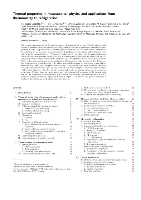
FIG. 1 Schematic picture of the system considered <strong>in</strong> this<br />
review. We describe an electron system <strong>in</strong> a diffusive wire,<br />
connected to two normal-metal or superconduct<strong>in</strong>g reservoirs<br />
via contacts of resistance RN . The reservoirs are further<br />
connected to the macroscopic measurement apparatus (see<br />
Subs. II.H). The heat flows <strong>and</strong> thermal conductances between<br />
the studied electron system <strong>and</strong> the external driv<strong>in</strong>g,<br />
the electromagnetic environment, <strong>and</strong> the phonons <strong>in</strong> the lattice<br />
(Subs. II.C <strong>and</strong> II.D) are <strong>in</strong>dicated with the arrows. The<br />
description of phonons <strong>in</strong> the lattice can further be divided <strong>in</strong><br />
the film phonons, substrate phonons <strong>and</strong> f<strong>in</strong>ally the heat bath<br />
on which the substrate resides (Subs. II.G). If the system is<br />
used as a radiation detector, it also couples to the radiation<br />
field, typically via some match<strong>in</strong>g circuit (Sec. IV).<br />
ma<strong>in</strong> methods used <strong>in</strong> the fabrication of mesoscopic electronic<br />
devices, <strong>and</strong> <strong>in</strong> Sec. VII we briefly discuss some of<br />
the ma<strong>in</strong> open questions <strong>in</strong> the field <strong>and</strong> the prospects<br />
of practical <strong>in</strong>struments based on electronic refrigeration<br />
<strong>and</strong> us<strong>in</strong>g the peculiar out-of-equilibrium energy distributions.<br />
II. THERMAL PROPERTIES OF MESOSCOPIC SCALE<br />
HYBRID STRUCTURES AT SUB-KELVIN<br />
TEMPERATURES<br />
The schematic picture of a setup studied <strong>in</strong> typical experiments<br />
described <strong>in</strong> this Review is shown <strong>in</strong> Fig. 1.<br />
The ma<strong>in</strong> object is a diffusive metal or heavily-doped<br />
semiconductor wire connected to large electrodes act<strong>in</strong>g<br />
as reservoirs where electrons thermalize quickly to the<br />
surround<strong>in</strong>gs. The electrons <strong>in</strong> the wire <strong>in</strong>teract between<br />
themselves, <strong>and</strong> are coupled to the phonons <strong>in</strong> the film<br />
<strong>and</strong> to the radiation <strong>and</strong> the fluctuations <strong>in</strong> the electromagnetic<br />
environment. The temperature Tph of the film<br />
phonons can, <strong>in</strong> a non-equilibrium situation, differ from<br />
that of the substrate phonons, Tsub <strong>and</strong> this can even differ<br />
from the phonon temperature T0 <strong>in</strong> the sample holder<br />
that is externally cooled. Under the applied voltage, the<br />
energy distribution function f(E) of electrons depends<br />
on each of these coupl<strong>in</strong>gs, <strong>and</strong> on the state (e.g., super-<br />
2<br />
E
conduct<strong>in</strong>g or normal) of the various parts of the system.<br />
In certa<strong>in</strong> cases detailed below, f(E) is a Fermi function<br />
feq(E; Te, µ) =<br />
1<br />
, (1)<br />
exp[(E − µ)/(kBTe)] + 1<br />
characterized by an electron temperature Te <strong>and</strong> potential<br />
µ. One of the ma<strong>in</strong> goals of this review is to expla<strong>in</strong><br />
how Te, <strong>and</strong> <strong>in</strong> some cases also Tph, can be driven even<br />
much below the lattice temperature T0, <strong>and</strong> how this low<br />
Te can be exploited to improve the sensitivity of applications<br />
rely<strong>in</strong>g on the electronic degrees of freedom. We<br />
also detail some of the out-of-equilibrium effects, where<br />
f(E) is not of the form of Eq. (1). In some setups, the<br />
specific form of f(E) can be utilized for novel physical<br />
phenomena.<br />
Throughout the Review, we concentrate on wires<br />
whose dimensions are large enough to fall <strong>in</strong> the quasiclassical<br />
diffusive limit. This means that the Fermi wavelength<br />
λF , elastic mean free path ℓel <strong>and</strong> the length of<br />
the wire L have to satisfy λF ≪ lel ≪ L. In this regime,<br />
the electron energy distribution function is well def<strong>in</strong>ed,<br />
<strong>and</strong> its space dependence can be described by a diffusion<br />
equation (Eq. (3)). In most parts of the Review, we assume<br />
the capacitances C of the contacts large enough,<br />
such that the charg<strong>in</strong>g energy EC = e 2 /2C is less than<br />
any of the relevant energy scales <strong>and</strong> can thus be ignored.<br />
Our approach is to describe the electron energy distribution<br />
function f(r, E) at a given position r of the sample<br />
<strong>and</strong> then relate this function to the charge <strong>and</strong> heat currents<br />
<strong>and</strong> their noise. In typical metal structures <strong>in</strong> the<br />
absence of superconductivity, phase-coherent effects are<br />
weak <strong>and</strong> often it is enough to rely on a semiclassical<br />
description. In this case, f(r, E) is described by a diffusion<br />
equation, as discussed <strong>in</strong> Subs. II.A. The electron<br />
reservoirs impose boundary conditions for the distribution<br />
functions, specified <strong>in</strong> Subs. II.B. The presence of<br />
<strong>in</strong>elastic scatter<strong>in</strong>g due to electron-electron <strong>in</strong>teraction,<br />
phonons or the electromagnetic environment can be described<br />
by source <strong>and</strong> s<strong>in</strong>k terms <strong>in</strong> the diffusion equation,<br />
specified by the collision <strong>in</strong>tegrals <strong>and</strong> discussed <strong>in</strong><br />
Subs. II.C. In the limit when these scatter<strong>in</strong>g effects are<br />
strong, the distribution function tends to a Fermi function<br />
feq(E; Te(r), µ(r)) throughout the wire, with a position<br />
dependent potential µ(r) <strong>and</strong> temperature Te(r).<br />
In this quasiequilibrium case, detailed <strong>in</strong> Subs. II.D, it<br />
thus suffices to f<strong>in</strong>d these two quantities. F<strong>in</strong>ally, with<br />
the knowledge of f(r; E), one can obta<strong>in</strong> the observable<br />
currents <strong>and</strong> their noise as described <strong>in</strong> Subs. II.E.<br />
In many cases, it is not enough to only describe the<br />
electrons <strong>in</strong>side the mesoscopic wire, assum<strong>in</strong>g that the<br />
surround<strong>in</strong>gs are totally unaffected by the changes <strong>in</strong> this<br />
electron system. If the phonons <strong>in</strong> the film are not well<br />
coupled to a large phonon bath, their temperature is <strong>in</strong>fluenced<br />
by the coupl<strong>in</strong>g to the electrons. In this case, it<br />
is important to describe the phonon heat<strong>in</strong>g or cool<strong>in</strong>g <strong>in</strong><br />
detail (see Subs. II.G). Often also the electron reservoirs<br />
may get heated due to an applied bias voltage, which<br />
has to be taken <strong>in</strong>to account <strong>in</strong> the boundary conditions.<br />
This heat<strong>in</strong>g is discussed <strong>in</strong> Subs. II.H.<br />
At the temperature range considered <strong>in</strong> this Review,<br />
many metals undergo a transition to the superconduct<strong>in</strong>g<br />
state (T<strong>in</strong>kham, 1996). This gives rise to several new<br />
phenomena that can be exploited, for example, for thermometry<br />
(see Sec. III), for radiation detection (Sec. IV)<br />
<strong>and</strong> for electron cool<strong>in</strong>g (Sec. V). The presence of superconductivity<br />
modifies both the diffusion equation (<strong>in</strong>side<br />
normal-metal wires through the proximity effect,<br />
see Subs. II.A) <strong>and</strong> especially the boundary conditions<br />
(Subs. II.B). Also the relations between the observable<br />
currents <strong>and</strong> the distribution functions are modified<br />
(Subs. II.E).<br />
Once the basic equations for f<strong>in</strong>d<strong>in</strong>g f(r, E) are outl<strong>in</strong>ed,<br />
we detail its behavior <strong>in</strong> different types of normalmetal<br />
– superconductor heterostructures <strong>in</strong> Subs. II.F.<br />
A. Boltzmann equation <strong>in</strong> a diffusive wire<br />
The semiclassical Boltzmann equation (Ashcroft <strong>and</strong><br />
Merm<strong>in</strong>, 1976; Smith <strong>and</strong> Jensen, 1989) describes the<br />
average number of particles, f(r, p)drdp/(2π) 3 , <strong>in</strong> the<br />
element {dr, dp} around the po<strong>in</strong>t {r, p} <strong>in</strong> the sixdimensional<br />
position-momentum space. The k<strong>in</strong>etic<br />
equation for f(r, p) is a cont<strong>in</strong>uity equation for particle<br />
flow,<br />
<br />
∂<br />
∂t + v · ∂r<br />
<br />
+ eE · ∂p f(r, p; t) = Iel[f] + I<strong>in</strong>[f]. (2)<br />
Here E is the electric field driv<strong>in</strong>g the charged particles<br />
<strong>and</strong> the elastic <strong>and</strong> <strong>in</strong>elastic collision <strong>in</strong>tegrals Iel <strong>and</strong><br />
I<strong>in</strong>, functionals of f, act as source <strong>and</strong> s<strong>in</strong>k terms. They<br />
illustrate the fact that scatter<strong>in</strong>g breaks translation symmetries<br />
<strong>in</strong> space <strong>and</strong> time — the total particle numbers<br />
expressed through the momentum <strong>in</strong>tegrals of f still rema<strong>in</strong><br />
conserved.<br />
In the metallic diffusive limit, Eq. (2) may be simplified<br />
as follows (Nagaev, 1992; Rammer, 1998; Sukhorukov<br />
<strong>and</strong> Loss, 1999). The electric field term can be absorbed<br />
<strong>in</strong> the space derivative by the substitution E = εp + µ(r)<br />
<strong>in</strong> the argument of the distribution function, such that<br />
E describes both the k<strong>in</strong>etic εp <strong>and</strong> the potential energy<br />
µ of the electron. Therefore, we are only left with the<br />
full r-dependent derivative v · ∇f = v · ∂rf + eE · ∂pf<br />
on the left-h<strong>and</strong> side of Eq. (2). In the diffusive regime,<br />
one may concentrate on length scales much larger than<br />
the mean free path ℓel. There, the particles quickly lose<br />
the memory of the direction of their <strong>in</strong>itial momentum,<br />
<strong>and</strong> the distribution functions become nearly isotropic <strong>in</strong><br />
the direction of v. Therefore, we may exp<strong>and</strong> the distribution<br />
function f <strong>in</strong> the two lowest spherical harmonics<br />
<strong>in</strong> the dependence on ˆv ≡ v/v, f(ˆv) = f0 + ˆv · δf, <strong>and</strong><br />
make the relaxation-time approximation to the elastic<br />
collision <strong>in</strong>tegral with the elastic scatter<strong>in</strong>g time τ, i.e.,<br />
Iel = −ˆv · δf/τ. In the limit where the time dependence<br />
of the distribution function takes place <strong>in</strong> a much slower<br />
3
scale than τ, this yields the diffusion equation with a<br />
source term,<br />
(∂t − D∇ 2 r)f0(r; E, t) = I<strong>in</strong>[f0]. (3)<br />
Here we assume that the particles move with the Fermi<br />
velocity, i.e., v = vF ˆv. As a result, their diffusive motion<br />
is characterized by the diffusion constant D = v2 F τ/3. In<br />
what follows, we will ma<strong>in</strong>ly concentrate on the static<br />
limit, i.e., assume ∂tf0(r; E, t) = 0 <strong>and</strong> lift the subscript<br />
0 from the angle-<strong>in</strong>dependent part f0 of the distribution<br />
function.<br />
Equation (3) can also be derived rigorously from the<br />
microscopic theory through the use of the quasiclassical<br />
Keldysh formalism (Rammer <strong>and</strong> Smith, 1986). With<br />
such an approach, one can also take <strong>in</strong>to account superconduct<strong>in</strong>g<br />
effects, such as Andreev reflection (Andreev,<br />
1964b) <strong>and</strong> the proximity effect (Belzig et al., 1999). In<br />
the diffusive limit, one obta<strong>in</strong>s the Usadel equation (Usadel,<br />
1970), which <strong>in</strong> the static case is<br />
D<br />
σA ∇ · Ǐ = −iEˇτ3 + ˇ ∆(r) + ˇ Σ<strong>in</strong>(r), ˇ G(r; E) . (4)<br />
Here ˇ G(r; E) is the isotropic part of the Keldysh Green’s<br />
function <strong>in</strong> the Keldysh ⊗ Nambu space, A <strong>and</strong> σ are<br />
the cross section <strong>and</strong> the normal-state conductivity of the<br />
wire, ˇτ3 = ˆ1⊗ˆτ3 is the third Pauli matrix <strong>in</strong> Nambu space,<br />
ˇ∆ = ˆ1⊗ ˆ ∆ is the pair potential matrix, <strong>and</strong> ˇ Σ<strong>in</strong> describes<br />
the <strong>in</strong>elastic scatter<strong>in</strong>g that is not conta<strong>in</strong>ed <strong>in</strong> ˇ ∆. Usadel<br />
equation describes the matrix current Ǐ = σA ˇ G∇ ˇ G<br />
(Nazarov, 1999), whose components <strong>in</strong>tegrated over the<br />
energy yield the physical currents. In the Keldysh space,<br />
ˇG is of the form<br />
<br />
ˆG R ˆK ˇG<br />
G<br />
=<br />
0 Gˆ A ,<br />
where each component is a 2 × 2 matrix <strong>in</strong> Nambu<br />
particle-hole space. Equation (4) has to be augmented<br />
with a normalization condition ˇ G 2 = 1. This implies<br />
( ˆ G R/A ) 2 = 1 <strong>and</strong> allows a parametrization ˆ G K =<br />
ˆG Rˆ h − ˆ h ˆ G A , where ˆ h is a distribution function matrix<br />
with two free parameters. The equations for the<br />
retarded/advanced functions ˆ G R/A ((1,1) <strong>and</strong> (2,2) -<br />
Keldysh components of Eq. (4)) describe the behavior of<br />
the pair<strong>in</strong>g amplitude. The solutions to these equations<br />
yield the coefficients for the k<strong>in</strong>etic equations, i.e., the<br />
(1,2) or the Keldysh part of Eq. (4). This describes the<br />
symmetric <strong>and</strong> antisymmetric parts of the energy distribution<br />
function with respect to the chemical potential of<br />
the superconductors. The latter is assumed everywhere<br />
equal to allow a time-<strong>in</strong>dependent description. A common<br />
choice is a diagonal ˆ h = f L + f T ˆτ3 (Schmid <strong>and</strong><br />
Schön, 1975), where f L (E) = f(−E) − f(E) is the antisymmetric<br />
<strong>and</strong> f T (E) = 1−f(E)−f(−E) the symmetric<br />
part of the energy distribution function f(E). With this<br />
choice, <strong>in</strong>side the normal metals where ˆ ∆ = 0, we get<br />
two k<strong>in</strong>etic equations of the form (Belzig et al., 1999;<br />
Virtanen <strong>and</strong> Heikkilä, 2004a)<br />
D∇ · j L = Σ L <strong>in</strong>, j L = σA(DL∇f L − T an ∇f T + jSf T ) ,<br />
(5a)<br />
D∇ · j T = Σ T <strong>in</strong>, j T = σA(DT ∇f T + T an ∇f L + jSf L ) .<br />
(5b)<br />
Here jL ≡ 1<br />
4Tr [(τ1 ⊗ ˆ1) Ǐ ] describes the spectral energy<br />
current, <strong>and</strong> jT ≡ 1<br />
4Tr [(τ1 ⊗ ˆτ3) Ǐ ] the spectral<br />
charge current. The <strong>in</strong>elastic effects are described by<br />
the collision <strong>in</strong>tegrals ΣL <strong>in</strong><br />
ΣT <strong>in</strong><br />
1 ≡ 4Tr [(τ1 ⊗ ˆ1)[ ˇ Σ<strong>in</strong>, ˇ G]] <strong>and</strong><br />
1 ≡ 4Tr [(τ1 ⊗ ˆτ3)[ ˇ Σ<strong>in</strong>, ˇ G]]. The k<strong>in</strong>etic coefficients are<br />
DL ≡ 1<br />
4 Tr [1− ˆ G R ˆ G A ]<br />
DT ≡ 1<br />
4 Tr [1− ˆ G R ˆτ3 ˆ G A ˆτ3]<br />
T an ≡ 1<br />
4 Tr [ ˆ G A ˆ G R ˆτ3]<br />
jS ≡ 1<br />
4 Tr [( ˆ G R ∇ ˆ G R − ˆ G A ∇ ˆ G A )ˆτ3].<br />
Here, DL <strong>and</strong> DT are the spectral energy <strong>and</strong> charge<br />
diffusion coefficients, <strong>and</strong> jS is the spectral density of<br />
the supercurrent-carry<strong>in</strong>g states (Heikkilä et al., 2002).<br />
The cross-term T an is usually small but not completely<br />
negligible. In a normal-metal wire <strong>in</strong> the absence of a<br />
proximity effect, ˆ G R = ˆτ3 <strong>and</strong> ˆ G A = − ˆτ3. Then we<br />
obta<strong>in</strong> DL = DT = 1, T an = jS = 0 <strong>and</strong> the k<strong>in</strong>etic<br />
equations (5b) reduce to Eq. (3) <strong>in</strong> the static limit.<br />
B. Boundary conditions<br />
The quasiclassical k<strong>in</strong>etic equations cannot directly describe<br />
constrictions whose size is of the order of the Fermi<br />
wavelength, such as tunnel junctions or quantum po<strong>in</strong>t<br />
contacts. However, such contacts can be described by<br />
the boundary conditions derived by Nazarov (1999),<br />
ǏL = ǏR = Z( 1<br />
2 { ˇ GL, ˇ GR})[ ˇ GR, ˇ GL], (6)<br />
where<br />
Z(x) = 2e2<br />
h<br />
<br />
n<br />
Tn<br />
2 + Tn(x − 1) .<br />
Here Ǐ L(R) <strong>and</strong> ˇ G L(R) are the matrix current <strong>and</strong> the<br />
Green’s function at the left (right) of the constriction,<br />
evaluated at the <strong>in</strong>terface <strong>and</strong> flow<strong>in</strong>g towards the right.<br />
The constriction is described by a set {Tn} of transmission<br />
eigenvalues through the function Z(x). For large<br />
constrictions, it is typically enough to transform the sum<br />
over the eigenvalues to an <strong>in</strong>tegral over the transmission<br />
probabilities T , weighted by their probability distribu-<br />
tion ρ(T ). In the case of a tunnel barrier, Tn ≪ 1,<br />
<strong>and</strong> thus Z(x) = 2e 2 /h <br />
n Tn ≡ GN /2. For a ballistic<br />
contact Tn ≡ 1 <strong>and</strong> Z(x) = GN/(x + 1). For<br />
4
other types of contacts, it is typically useful to f<strong>in</strong>d<br />
the observable for arbitrary T <strong>and</strong> weight it with ρ(T ),<br />
e.g., ρ(T ) = πGN /[(2e 2 )T √ 1 − T ] for a diffusive contact<br />
(Nazarov, 1994), ρ(T ) = GN /[e 2 T 3/2√ 1 − T ] for<br />
a dirty <strong>in</strong>terface (Schep <strong>and</strong> Bauer, 1997) or ρ(T ) =<br />
2GN/[e 2 T (1 − T )] for a chaotic cavity (Baranger <strong>and</strong><br />
Mello, 1994). This way, the observables can be related<br />
to the normal-state conductance GN of the junction.<br />
Equation (6) yields a boundary condition both for the<br />
”spectral” functions ˆ G R/A <strong>and</strong> for the distribution functions.<br />
In the absence of superconductivity, we simply<br />
have ˆ G R/A = ±ˆτ3, <strong>and</strong> the boundary condition for the<br />
distribution functions becomes <strong>in</strong>dependent of the type<br />
of the constriction,<br />
j L/T = GN (f L/T<br />
R<br />
L/T<br />
− fL ). (7)<br />
In this case, the two currents can be <strong>in</strong>cluded <strong>in</strong> the same<br />
function by def<strong>in</strong><strong>in</strong>g j(±E) = (j L (E) ± j T (E))/2. This<br />
yields the spectral current through the constriction<br />
j(E) = GN (fL(E) − fR(E)), (8)<br />
where f L/R is the energy distribution function on the<br />
left/right side of the constriction.<br />
Another <strong>in</strong>terest<strong>in</strong>g yet tractable case is the one where<br />
a superconduct<strong>in</strong>g reservoir (on the ”left” of the junction)<br />
is connected to a normal metal (on the ”right”)<br />
<strong>and</strong> the proximity effect <strong>in</strong>to the latter can be ignored.<br />
The latter is true, for example, if we are <strong>in</strong>terested <strong>in</strong> the<br />
distribution function at energies far exceed<strong>in</strong>g the Thouless<br />
energy of the normal-metal wire, or <strong>in</strong> the presence<br />
of strong depair<strong>in</strong>g. In this case, the spectral energy <strong>and</strong><br />
charge currents are<br />
j L = 2e2<br />
h<br />
j T = 2e2<br />
h<br />
<br />
TnML(Tn)θ( Ē)(f L R − f L L ) (9a)<br />
n<br />
<br />
Tn(M 1 T (Tn)θ(−Ē) + M 2 T (Tn)θ( Ē)f T R .<br />
n<br />
(9b)<br />
Here Ē = |E| − ∆ <strong>and</strong> θ(E) is the Heaviside step function,<br />
<strong>and</strong> the energy-dependent coefficients are<br />
ML(T ) = 2 (2 − T )|E|Ω + T Ω 2<br />
((2 − T )Ω + T |E|) 2<br />
M 1 T (T ) =<br />
M 2 T (T ) =<br />
2T ∆2 4(T − 1)E2 + (T − 2) 2∆2 2|E|<br />
(2 − T )Ω + T |E|<br />
(10a)<br />
(10b)<br />
(10c)<br />
Here we def<strong>in</strong>ed Ω ≡ √ E 2 − ∆ 2 . In the tunnel<strong>in</strong>g limit<br />
T ≪ 1, we get<br />
j L/T = NS(E)(f L/T<br />
R<br />
L/T<br />
− fL ), (11)<br />
where<br />
<br />
<br />
<br />
NS(E) = <br />
Re<br />
<br />
<br />
E + iΓ<br />
<br />
Γ→0<br />
→ θ(Ē)|E|/Ω<br />
(E + iΓ) 2 − ∆2 (12)<br />
is the reduced superconduct<strong>in</strong>g density of states (DOS).<br />
The first form of Eq. (12) assumes a f<strong>in</strong>ite pair-break<strong>in</strong>g<br />
rate Γ, which turns out to be relevant <strong>in</strong> some cases discussed<br />
<strong>in</strong> Sec. V.C.1 Unless specified otherwise, we assume<br />
that the superconductors are of the conventional<br />
weak-coupl<strong>in</strong>g type <strong>and</strong> the superconduct<strong>in</strong>g energy gap<br />
∆ at T = 0 is related to the critical temperature Tc by<br />
∆ ≈ 1.764kBTc (T<strong>in</strong>kham, 1996).<br />
C. Collision <strong>in</strong>tegrals for <strong>in</strong>elastic scatter<strong>in</strong>g<br />
The collision <strong>in</strong>tegral I<strong>in</strong> <strong>in</strong> Eq. (3) is due to electron–<br />
electron, electron–phonon <strong>in</strong>teraction <strong>and</strong> the <strong>in</strong>teraction<br />
with the photons <strong>in</strong> the electromagnetic environment.<br />
1. Electron-electron scatter<strong>in</strong>g<br />
For the electron–electron <strong>in</strong>teraction, the collision <strong>in</strong>tegral<br />
is of the form<br />
I e−e<br />
coll<br />
= κ(d)<br />
e−e<br />
<br />
dωdE ′ Ĩ<br />
α <strong>in</strong><br />
ω coll(ω, E, E ′ ) − Ĩout coll(ω, E, E ′ <br />
) ,<br />
5<br />
(13)<br />
where α <strong>and</strong> κ (d)<br />
e−e depend on the type of scatter<strong>in</strong>g <strong>and</strong><br />
the ”<strong>in</strong>” <strong>and</strong> ”out” collisions are<br />
Ĩ <strong>in</strong><br />
coll = [1 − f(E)][1 − f(E ′ )]f(E − ω)f(E ′ + ω)<br />
(14a)<br />
Ĩ out<br />
coll = f(E)f(E ′ )[1 − f(E − ω)][1 − f(E ′ + ω)].<br />
(14b)<br />
Electron-electron scatter<strong>in</strong>g can be either due to the direct<br />
Coulomb <strong>in</strong>teraction (Altshuler <strong>and</strong> Aronov, 1985),<br />
or mediated through magnetic impurities which can flip<br />
their sp<strong>in</strong> <strong>in</strong> a scatter<strong>in</strong>g process (Kam<strong>in</strong>ski <strong>and</strong> Glazman,<br />
2001) or other types of impurities with <strong>in</strong>ternal dynamics.<br />
In practice, both of these effects contribute to<br />
the energy relaxation (Anthore et al., 2003; Pierre et al.,<br />
2000). Assum<strong>in</strong>g the electron–electron <strong>in</strong>teraction is local<br />
on the scale of the variations <strong>in</strong> the distribution function,<br />
the direct <strong>in</strong>teraction yields (Altshuler <strong>and</strong> Aronov,<br />
1985) Eq. (13) with α = −2 + d/2 for a d-dimensional<br />
wire. In a diffusive wire, the effective dimensionality of<br />
the wire is determ<strong>in</strong>ed by compar<strong>in</strong>g the dimensions to<br />
the energy-dependent length LE ≡ D/E. The pref-
actor κ (d)<br />
e−e for a d-dimensional sample is<br />
κ (1)<br />
e−e =<br />
1<br />
π √ 2D2 , (Huard et al., 2004) (15a)<br />
νF A<br />
κ (2)<br />
e−e = 1<br />
, (Rammer <strong>and</strong> Smith, 1986) (15b)<br />
8EF τ<br />
κ (3)<br />
e−e =<br />
1<br />
8π2√22 , (Rammer, 1998) (15c)<br />
νF D3/2 where νF = ν(EF ) is the density of states at the Fermi<br />
energy EF <strong>and</strong> A is the wire cross-section.<br />
In the case of relaxation due to magnetic impurities,<br />
one expects (Kam<strong>in</strong>ski <strong>and</strong> Glazman, 2001) α = −2 <strong>and</strong><br />
κe−e = π<br />
2<br />
cm S(S + 1)<br />
νF<br />
<br />
ln<br />
eV<br />
kBTK<br />
−4<br />
. Here cm is the<br />
concentration, S is the sp<strong>in</strong>, <strong>and</strong> TK is the Kondo temperature<br />
of the magnetic impurities responsible for the<br />
scatter<strong>in</strong>g. This form is valid for T > TK. For a more<br />
detailed account of the magnetic-impurity effects, see<br />
(Göppert et al., 2002; Göppert <strong>and</strong> Grabert, 2001, 2003;<br />
Kroha <strong>and</strong> Zawadowski, 2002; Ujsaghy et al., 2004) <strong>and</strong><br />
the references there<strong>in</strong>.<br />
For d = 3, <strong>and</strong> for small deviations δf from<br />
equilibrium, the collision <strong>in</strong>tegral can be approxi-<br />
mated (Rammer, 1998) by −δf/τe−e, where τe−e =<br />
3 √ 3π( √ 8−1)ζ(3/2)(kBT ) 3/2 √<br />
/(16kF ℓel τEF ) is the relaxation<br />
time (ζ(3/2) ≈ 2.612), τ = ℓel/vF is the elastic<br />
scatter<strong>in</strong>g time <strong>and</strong> kF is the Fermi momentum. In the<br />
case when α < −1/2, the usual relaxation-time approach<br />
does not work for the electron–electron <strong>in</strong>teraction as<br />
the expression for the relaxation time has an <strong>in</strong>frared divergence<br />
(Altshuler <strong>and</strong> Aronov, 1985; Rammer, 1998).<br />
Therefore, one has to solve the full Boltzmann equation<br />
with the proper collision <strong>in</strong>tegrals. To obta<strong>in</strong> an estimate<br />
for the length scale at which the electron–electron <strong>in</strong>teraction<br />
is effective, we can proceed differently. Introduc<strong>in</strong>g<br />
dimensionless position ˜x ≡ x/L <strong>and</strong> energy variables<br />
˜E ′ ≡ E ′ /E∗ <strong>and</strong> ˜ω ≡ ω/E∗ , we get<br />
∂ 2 ˜xf = −Ke−e Ĩcoll.<br />
Here the dimensionless <strong>in</strong>tegral Ĩcoll characterizes the deviation<br />
<strong>in</strong> the shape of the distribution function from the<br />
Fermi function <strong>and</strong> Ke−e depends on the specific system.<br />
For a quasi-1d wire with bare Coulomb <strong>in</strong>teraction,<br />
Ke−e = 1<br />
√<br />
2<br />
RD<br />
RK<br />
<br />
E∗ , (16)<br />
where RK = h/(2e 2 ), RD = L/(σA) is the resistance<br />
of the wire <strong>and</strong> ET = D/L 2 is the Thouless energy.<br />
In the case when the wire term<strong>in</strong>ates <strong>in</strong> a po<strong>in</strong>t contact<br />
with resistance RT , the resistance RD <strong>in</strong> Eq. (16) should<br />
be replaced with the total resistance RD + RT (Pekola<br />
et al., 2004a). Typically the energy scale characteriz<strong>in</strong>g<br />
the deviation from (quasi)equilibrium is E ∗ = eV . At<br />
eV ≫ kBT , electron–electron collisions start to be effec-<br />
ET<br />
tive when Ke−e ≈ 1. This yields a length scale<br />
ℓ ∗ <br />
<br />
2D<br />
e−e = RKAσ , (17)<br />
eV<br />
where A is the cross section of the wire <strong>and</strong> σ its conductivity.<br />
Us<strong>in</strong>g a wire with resistance RD = 10 Ω <strong>and</strong><br />
ET ≈ 10 µeV for L = 1 µm (close to the values <strong>in</strong><br />
(Huard et al., 2004)), <strong>and</strong> a voltage V = 100 µV, we get<br />
ℓ ∗ e−e ≈ 24 µm. Increas<strong>in</strong>g the temperature, Ĩcoll becomes<br />
smaller, <strong>and</strong> this effective length also decreases. The experimental<br />
results of Huard et al. (2004) <strong>in</strong>dicate at least<br />
an order of magnitude larger κe−e <strong>and</strong> thus smaller ℓ ∗ e−e<br />
than predicted by this theory. At present, the reasons<br />
for this discrepancy have not been found.<br />
2. Electron–phonon scatter<strong>in</strong>g<br />
Another source of <strong>in</strong>elastic scatter<strong>in</strong>g is due to<br />
phonons, for which the collision <strong>in</strong>tegral is of the form<br />
(Rammer, 1998; Wellstood et al., 1994)<br />
I e−ph<br />
coll<br />
= 2π<br />
∞<br />
0<br />
dωα 2 <br />
<strong>in</strong><br />
F (ω) Ĩcoll(E, ω) − Ĩout<br />
<br />
coll(E, ω) .<br />
Here<br />
Ĩ <strong>in</strong><br />
coll(E, ω) =f(E + ω)[1 − f(E)][1 + nph(ω)]<br />
+ [1 − f(E)]f(E − ω)nph(ω))<br />
Ĩ out<br />
coll(E, ω) =f(E)[1 − f(E − ω)][1 + nph(ω)]<br />
+ f(E)[1 − f(E + ω)]nph(ω).<br />
6<br />
(18)<br />
(19)<br />
The kernel α 2 F (ω) (the Eliashberg function) of the <strong>in</strong>teraction<br />
depends on the type of considered phonons<br />
(longitud<strong>in</strong>al or transverse), on the relation between the<br />
phonon wavelength λph <strong>and</strong> the electron mean free path<br />
ℓel, on the dimensionality of the electron <strong>and</strong> phonon<br />
system (Sergeev et al., 2005), <strong>and</strong> on the characteristics<br />
of the Fermi surface (Prunnila et al., 2005). At<br />
sub-kelv<strong>in</strong> temperatures <strong>and</strong> low voltages, the optical<br />
phonons can be neglected, <strong>and</strong> one can only concentrate<br />
on the acoustic phonons. In what follows, we also neglect<br />
phonon quantization effects which may be important <strong>in</strong><br />
restricted geometries. Moreover, the phonon distribution<br />
function nph(ω) is considered to be <strong>in</strong> (quasi)equilibrium,<br />
i.e., described by a Bose distribution function nph(ω) =<br />
neq(ω) ≡ [exp(ω/(kBT )) − 1] −1 (for phonon relaxation<br />
processes, see Subs. II.G).<br />
When the phonon temperature Tph is much lower than<br />
the Debye temperature TD, the phonon dispersion relation<br />
is l<strong>in</strong>ear <strong>and</strong> one can estimate the phonon wavelength<br />
us<strong>in</strong>g λph = hvS/kBTph. For typical metals, the speed<br />
of sound is vS ∼ 3 . . . 5 km/s, which yields a wavelength<br />
λph ∼ 100 . . . 200 nm at Tph = 1 K <strong>and</strong> λph ∼ 1 . . . 2 µm<br />
at Tph = 100 mK. In the clean limit λph ≪ ℓel, approximat<strong>in</strong>g<br />
the electron-phonon coupl<strong>in</strong>g with a scalar deformation<br />
potential, only the longitud<strong>in</strong>al phonons are coupled<br />
to the electrons. In this case for ω ≪ kBTD/, kF vS
Te (mK) Tph Σ (W<br />
(mK) m −3 K −5 Measured <strong>in</strong><br />
)<br />
Ag 50...400 50...400 0.5 10 9<br />
(Ste<strong>in</strong>bach et al., 1996)<br />
Al 35...130 35 0.2 10 9<br />
(Kautz et al., 1993)<br />
200...300 200 0.3 10 9<br />
(Meschke et al., 2004)<br />
Au 80...1200 80...1000 2.4 10 9<br />
(Echternach<br />
1992)<br />
et al.,<br />
AuCu 50...120 20...120 2.4 10 9<br />
(Wellstood et al., 1989)<br />
Cu 25...800 25...320 2.0 10 9<br />
(Roukes et al., 1985)<br />
100...500 280...400 0.9...4 10 9 (Leivo et al., 1996)<br />
50...200 50...150 2.0 10 9<br />
(Meschke et al., 2004)<br />
Mo 980 80...980 0.9 10 9<br />
(Sav<strong>in</strong><br />
2005)<br />
<strong>and</strong> Pekola,<br />
n ++ Si 120...400 175...400 0.1 10 9<br />
(Sav<strong>in</strong> et al., 2001)<br />
173...450 173 0.04 10 9<br />
(Prunnila et al., 2002)<br />
320...410 320...410 0.1 10 9<br />
(Buonomo et al., 2003)<br />
Ti 300...800 500...800 1.3 10 9<br />
(Mann<strong>in</strong>en et al., 1999)<br />
TABLE I Measured electron-phonon coupl<strong>in</strong>g constant Σ for<br />
different materials. The second <strong>and</strong> third columns <strong>in</strong>dicate<br />
the temperature ranges (electron <strong>and</strong> phonon temperatures,<br />
respectively) of the measurements.<br />
(Rammer, 1998; Wellstood et al., 1994)<br />
|M| 2<br />
α 2 F (ω) =<br />
4π22v 3 SνF ω 2 , (20)<br />
where |M| 2 is the square of the matrix element for the<br />
deformation potential. Generally this is <strong>in</strong>versely proportional<br />
to the mass density of the ions, but its precise<br />
microscopic form depends on the details of the lattice<br />
structure. Therefore it is useful to present |M| <strong>in</strong><br />
terms of a separately measurable quantity, e.g., the prefactor<br />
Σ of the power P = ΣVT 5 dissipated to the lattice<br />
of volume V <strong>in</strong> the quasiequilibrium limit (see Table<br />
I <strong>and</strong> Subs. II.D): |M| 2 = π5v3 SΣ/(12ζ(5)k5 B ), where<br />
ζ(5) ≈ 1.0369.<br />
In the dirty limit λph ≫ ℓel, the power of ω <strong>in</strong> the<br />
Eliashberg function can be either 1 or 3, for the cases<br />
of static or vibrat<strong>in</strong>g disorder, respectively. For further<br />
details about the dirty limit, we refer to (Belitz, 1987;<br />
Rammer <strong>and</strong> Schmid, 1986; Sergeev <strong>and</strong> Mit<strong>in</strong>, 2000).<br />
The relaxation rate for electron-phonon scatter<strong>in</strong>g is<br />
given by 1/τe−ph = −{δIe−ph[f(E)]/δf(E)}| f(E)=feq(E),<br />
where feq(E) now is a Fermi function at the lattice temperature.<br />
With this def<strong>in</strong>ition at E = EF , (Rammer,<br />
1998)<br />
1<br />
τe−ph<br />
= 4π<br />
∞<br />
0<br />
dω α2F (ω)<br />
.<br />
s<strong>in</strong>h<br />
(21)<br />
ω<br />
kBT<br />
Thus, <strong>in</strong> the clean case for kBT ≪ 2kF vS we obta<strong>in</strong><br />
1/τe−ph = αT 3 , α = 7ζ(3)Σ/(24ζ(5)k 2 B νF ) ≈<br />
0.34Σ/(k 2 B νF ). With typical values for Cu, Σ = 2 · 10 9<br />
WK −5 m −3 <strong>and</strong> νF = 1.6·10 47 J −1 m −3 , we get τe−ph = 45<br />
ns at T = 1 K. Assum<strong>in</strong>g λF ≪ ℓel ≪ ℓe−ph, the<br />
electron–phonon scatter<strong>in</strong>g length is ℓe−ph = Dτe−ph.<br />
For the above values <strong>and</strong> a typical diffusion constant<br />
D = 0.01 m 2 /s, ℓe−ph ≈ 21 µm at T = 1 K <strong>and</strong><br />
ℓe−ph ≈ 670 µm at T = 100 mK.<br />
In the disordered limit λph ≫ lel, the temperature dependence<br />
of the electron-phonon scatter<strong>in</strong>g rate is expected<br />
to follow either the T 2 or T 4 laws, depend<strong>in</strong>g on<br />
the nature of the disorder (Sergeev <strong>and</strong> Mit<strong>in</strong>, 2000).<br />
It seems that although most of the experiments are<br />
done <strong>in</strong> the limit where the phonon wavelength at least<br />
slightly exceeds the electron mean free path, <strong>in</strong> majority<br />
of the cases the results have fitted to the clean-limit expressions,<br />
i.e., the scatter<strong>in</strong>g rate ∝ T 3 e <strong>and</strong> the heat current<br />
flow<strong>in</strong>g <strong>in</strong>to the phonon system ∝ T 5 e , see Eq. (24)<br />
below (for an exception, see (Karvonen et al., 2005)).<br />
F<strong>in</strong>d<strong>in</strong>g the correct exponent is not straightforward, as<br />
the film phonons are also typically affected by the measurement,<br />
<strong>and</strong> because of the reduced dimensionality of<br />
the phonon system (see Subs. II.G). In this Review, we<br />
concentrate on the clean-limit expressions.<br />
D. Quasiequilibrium limit<br />
The shape of the distribution function at a given position<br />
of the wire strongly depends on how the <strong>in</strong>elastic<br />
scatter<strong>in</strong>g length l<strong>in</strong> compares to the length L of the<br />
wire. For L ≪ l<strong>in</strong> (nonequilibrium limit), we may neglect<br />
the <strong>in</strong>elastic scatter<strong>in</strong>g altogether. In this case, the<br />
distribution function is a solution to either Eqs. (5) or<br />
Eq. (3), where the collision <strong>in</strong>tegrals/self energies for <strong>in</strong>elastic<br />
scatter<strong>in</strong>g can be neglected. As a result, the shape<br />
of the electron distribution functions <strong>in</strong>side the wire at a<br />
f<strong>in</strong>ite bias voltage eV kBT may strongly deviate from a<br />
Fermi distribution (Giazotto et al., 2004b; Heikkilä et al.,<br />
2003; Hesl<strong>in</strong>ga <strong>and</strong> Klapwijk, 1993; Pekola et al., 2004a;<br />
Pierre et al., 2001; Pothier et al., 1997b). The nonequilibrium<br />
shape shows up <strong>in</strong> most of the observable <strong>properties</strong><br />
of the system, <strong>in</strong>clud<strong>in</strong>g the I − V characteristics,<br />
the current noise or the supercurrent. In general, it can<br />
only be neglected <strong>in</strong> the I −V characteristics if the charge<br />
transport process is energy <strong>in</strong>dependent as <strong>in</strong> the case of<br />
purely normal-metal samples. Even <strong>in</strong> this case the form<br />
of f(E) can be observed <strong>in</strong> the current noise.<br />
The k<strong>in</strong>etic equations can be greatly simplified <strong>in</strong> the<br />
limit where ℓ<strong>in</strong> for one type of scatter<strong>in</strong>g is much smaller<br />
than L. In the quasiequilibrium limit, the energy relaxation<br />
length due to electron–electron scatter<strong>in</strong>g is much<br />
shorter than the wire, ℓe−e ≪ L (Nagaev, 1995). In this<br />
case, the local distribution function is a Fermi function<br />
characterized by the temperature Te(r, t) <strong>and</strong> potential<br />
µ(r, t). Mathematically, this can be seen by consider<strong>in</strong>g<br />
the Boltzmann equation (3) with the electron–electron<br />
collision <strong>in</strong>tegral, Eq. (13) <strong>in</strong> the limit where the prefactor<br />
of the latter becomes very large. As the left-h<strong>and</strong><br />
side of Eq. (3) is not strongly dependent on the form of<br />
f(E, r) as a function of energy, the equation can only<br />
be satisfied if the collision <strong>in</strong>tegral without the prefactor<br />
becomes small. It can be easily shown that the latter<br />
7
vanishes for f(E) = feq(E). Thus, the deviations from<br />
the Fermi-function shape will be at most of the order of<br />
ℓ<strong>in</strong>/L, <strong>and</strong> can be neglected <strong>in</strong> the quasiequilibrium limit.<br />
In this limit, we are still left with two unknowns,<br />
Te(r, t) <strong>and</strong> µ(r, t). Substitut<strong>in</strong>g f(E, r) =<br />
feq(E; Te(r, t), µ(r, t)) <strong>in</strong> Eq. (3) yields<br />
(∂t − D∇ 2 )f = (∂t − D∇ 2 )(Te∂Tef + µ∂µf)−<br />
D[(∇µ) 2 ∂ 2 µf) + (∇Te) 2 ∂ 2 Te f + 2∇Te∇µ∂Te∂µf] = Icoll[f],<br />
where Icoll[f] conta<strong>in</strong>s the other types of <strong>in</strong>elastic scatter<strong>in</strong>gs,<br />
e.g., those with the phonons. In the right h<strong>and</strong> side<br />
of the upper l<strong>in</strong>e, the differential operators ∂t <strong>and</strong> ∇ act<br />
only on Te <strong>and</strong> µ. Integrat<strong>in</strong>g this over the energy <strong>and</strong><br />
multiply<strong>in</strong>g by νF E <strong>and</strong> then <strong>in</strong>tegrat<strong>in</strong>g over E yields<br />
(∂t − D∇ 2 )µ(r) = 0, (22)<br />
Ce(r, t)∂tTe − ∇(κ(r, t)∇Te) − σ(∇µ/e) 2 = Ĩcoll. (23)<br />
We assumed that the energy <strong>in</strong>tegral over Icoll[f] vanishes.<br />
1 Here Ce(r, t) = π 2 νF k 2 B Te(r, t)/3 is the electron<br />
heat capacity, σ = DνF e 2 is the Drude conductivity,<br />
κ(r, t) = σL0Te(r, t) is the electron heat conductivity,<br />
L0 = π 2 k 2 B /(3e2 ) ≈ 2.45 · 10 −8 WΩK −2 is the Lorenz<br />
number <strong>and</strong> Ĩcoll(Te, µ) conta<strong>in</strong>s the power per unit volume<br />
emitted or absorbed by other excitations, such as<br />
phonons or the electromagnetic radiation field. The last<br />
term on the left h<strong>and</strong> side of Eq. (23) describes the Joule<br />
heat<strong>in</strong>g due to the applied voltage. In what follows,<br />
we write the volume explicitly <strong>in</strong> the collision <strong>in</strong>tegral<br />
by averag<strong>in</strong>g over a small volume V around the po<strong>in</strong>t<br />
r where T (r) is approximately constant, thus def<strong>in</strong><strong>in</strong>g<br />
Pcoll(r) ≡ V Ĩcoll.<br />
For the electron-phonon scatter<strong>in</strong>g (Wellstood et al.,<br />
1994), Pcoll reads <strong>in</strong> the clean case (see also Table I)<br />
P e−ph<br />
coll = ΣV(Te(r) 5 − Tph(r) 5 ). (24)<br />
For the dirty limit specified below Eq. (20), the Eliashberg<br />
functions scal<strong>in</strong>g with ω n translate <strong>in</strong>to temperature<br />
dependences scal<strong>in</strong>g as T n+3 , i.e., T 4 <strong>and</strong> T 6 (Sergeev<br />
<strong>and</strong> Mit<strong>in</strong>, 2000).<br />
The electrons can also be heated due to the thermal<br />
noise <strong>in</strong> their electromagnetic environment unless proper<br />
filter<strong>in</strong>g is realized to prevent this heat<strong>in</strong>g. If one aims<br />
to detect the electromagnetic environment as discussed <strong>in</strong><br />
Sec. IV, this discussion can of course be turned around to<br />
f<strong>in</strong>d the optimal coupl<strong>in</strong>g to the radiation to be observed.<br />
A model for such coupl<strong>in</strong>g <strong>in</strong> the quasiequilibrium limit<br />
was considered by Schmidt et al. (2004a), who obta<strong>in</strong>ed<br />
an expression for the emitted/absorbed power due to the<br />
external noise <strong>in</strong> the form<br />
P e−em<br />
coll<br />
= r k2 B π2<br />
6h (T 2 e − T 2 γ ). (25)<br />
1 In the diffusive limit where the <strong>in</strong>elastic scatter<strong>in</strong>g rates are lower<br />
than 1/τ, this is related to the particle number conservation <strong>and</strong><br />
is thus generally valid.<br />
Here r = 4ReRγ/(Re + Rγ) 2 is the coupl<strong>in</strong>g constant,<br />
Tγ is the (noise) temperature of the environment, <strong>and</strong><br />
Re <strong>and</strong> Rγ are the resistances characteriz<strong>in</strong>g the thermal<br />
noise <strong>in</strong> the electron system <strong>and</strong> the environment,<br />
respectively. This expression assumes a frequency <strong>in</strong>dependent<br />
environment <strong>in</strong> the relevant frequency range.<br />
For some examples on the frequency dependence, we refer<br />
to Schmidt et al. (2004a).<br />
E. Observables<br />
1. Currents<br />
In the nonequilibrium diffusive limit, the charge current<br />
<strong>in</strong> a normal-metal wire <strong>in</strong> the absence of a proximity<br />
effect or any such <strong>in</strong>terference effects as weak localization<br />
is obta<strong>in</strong>ed from the local distribution function by<br />
I = −eA<br />
∞<br />
−∞<br />
dED(E)ν(E)∇f(x; E) (26)<br />
<strong>and</strong> the heat current from a reservoir with potential µ is<br />
˙Q = −A<br />
∞<br />
−∞<br />
dE(E − µ)D(E)ν(E)∇f(x; E). (27)<br />
Here we <strong>in</strong>cluded the possible energy dependence of the<br />
diffusion constant D(E) <strong>and</strong> of the density of states ν(E),<br />
due to the energy dependence of the elastic scatter<strong>in</strong>g<br />
time, or due to the nonl<strong>in</strong>earities <strong>in</strong> the quasiparticle dispersion<br />
relation. If the Kondo effect (Vavilov et al., 2003)<br />
can be neglected, such effects are very small <strong>in</strong> good metals<br />
at temperatures of the order of 1 K or less.<br />
In the quasiequilibrium limit, assum<strong>in</strong>g D(E) =const.<br />
<strong>and</strong> ν(E) = νF , Eqs. (26,27) can be simplified to<br />
8<br />
I = −σA∇µ/e (28a)<br />
˙Q = −κA∇T. (28b)<br />
When a diffusive wire of resistance RD is connected<br />
to a reservoir through a po<strong>in</strong>t contact characterized by<br />
the transmission eigenvalues {Tn}, the f<strong>in</strong>al distribution<br />
function is obta<strong>in</strong>ed after solv<strong>in</strong>g the Boltzmann equation<br />
(3) or Eqs. (5) with the boundary conditions given by<br />
Eq. (6), (8), or by (9). However, when RD is much less<br />
than the normal-state resistance 1/GN of the contact,<br />
we can ignore the wire <strong>and</strong> obta<strong>in</strong> the full current by a<br />
direct <strong>in</strong>tegration over Eq. (8) or Eq. (9). For example,<br />
for NIS or SIS tunnel junctions, the expressions for the<br />
charge <strong>and</strong> heat currents from the left side of the junction<br />
become<br />
I = 1<br />
eRT<br />
˙Q = 1<br />
e2RT <br />
dENL( ˜ E)NR(E)[fL(E) − fR(E)] (29)<br />
<br />
dE ˜ ENL( ˜ E)NR(E)[fL(E) − fR(E)]. (30)<br />
Here ˜ E = E − eV , RT = 1/GN , N L/R(E) = ν(E)/νF<br />
is the reduced density of states for the left/right wire,
N(E) = 1 for a normal metal <strong>and</strong> N(E) = NS(E) for a<br />
superconductor. Furthermore, if the two wires constitute<br />
reservoirs, fL/R are Fermi functions with potentials µL =<br />
−eV , µR = 0. The result<strong>in</strong>g NIS or SIS charge current is<br />
a sensitive probe of temperature <strong>and</strong> can hence be used<br />
for thermometry or radiation detection, as expla<strong>in</strong>ed <strong>in</strong><br />
Secs. III.A <strong>and</strong> IV, respectively. Moreover, analysis of<br />
the heat current Eq. (30) shows that the electrons can<br />
<strong>in</strong> certa<strong>in</strong> situations be cooled <strong>in</strong> NIS/SIS structures, as<br />
discussed <strong>in</strong> Sec. V.C.1.<br />
In the presence of a proximity effect, the equations<br />
for the charge <strong>and</strong> thermal currents <strong>in</strong> the quasiclassical<br />
limit, i.e., ignor<strong>in</strong>g the energy dependence of the diffusion<br />
constant <strong>and</strong> the normal-metal density of states, are<br />
<br />
I = dEj T<br />
(31a)<br />
<br />
˙Q = dE(Ej L − µj T ). (31b)<br />
Here µ is the potential of the reservoir from which the<br />
heat current is calculated. As <strong>in</strong> Eq. (5), these currents<br />
can be separated <strong>in</strong>to quasiparticle, anomalous, <strong>and</strong> supercurrent<br />
parts.<br />
2. Noise<br />
Often one can express the zero-frequency current noise<br />
<strong>in</strong> terms of the local distribution function (Blanter <strong>and</strong><br />
Büttiker, 2000). The noise is characterized by the correlator<br />
∞<br />
S = 2 dt<br />
−∞<br />
′ 〈δÎ(t + t′ )δÎ(t)〉, where δÎ = Î − 〈Î〉 <strong>and</strong> Î is the current operator. In a<br />
stationary system S is <strong>in</strong>dependent of t. In a normalmetal<br />
wire of length L <strong>in</strong> the nonequilibrium limit, the<br />
current noise S can be expressed as (Nagaev, 1992)<br />
S = 4eDνF A<br />
L 2<br />
L<br />
0<br />
∞<br />
dx dEf(E, x)[1 − f(E, x)]. (32)<br />
−∞<br />
In the quasiequilibrium regime, this equation simplifies<br />
to (Nagaev, 1995)<br />
S = 4eDνF AkB<br />
L 2<br />
L<br />
0<br />
dxTe(x). (33)<br />
When the resistance of a po<strong>in</strong>t contact dom<strong>in</strong>ates that<br />
of the wire, the noise power can be expressed through<br />
(Blanter <strong>and</strong> Büttiker, 2000)<br />
SNN = 2e2<br />
h<br />
<br />
<br />
dE{Tn [fL(1 − fL) + fR(1 − fR)]<br />
n<br />
+ Tn(1 − Tn)(fL − fR) 2 }<br />
for a normal-metal contact <strong>and</strong> (de Jong <strong>and</strong> Beenakker,<br />
1994)<br />
SNS = 2e2<br />
h<br />
<br />
<br />
n<br />
<br />
T<br />
dE<br />
2<br />
n<br />
(2 − Tn) 2 2fL(E)[1 − fL(E)]<br />
+ 16T 2<br />
n (1 − Tn)<br />
(2 − Tn) 4<br />
(f T L ) 2<br />
for an <strong>in</strong>coherent NS contact at E < ∆. Here f L/R<br />
are the distribution functions <strong>in</strong> the left/right (normal/superconduct<strong>in</strong>g<br />
<strong>in</strong> the latter case) side of the contact<br />
<strong>and</strong> f T L (E) = 1 − fL(E) − fL(−E), the symmetric<br />
part w.r.t. the S potential. If the scatter<strong>in</strong>g probabilities<br />
are <strong>in</strong>dependent of energy <strong>and</strong> if the two sides are<br />
reservoirs with the same temperature, these expressions<br />
simplify to<br />
SNN = 2e2<br />
h<br />
SNS = 2e2<br />
h<br />
+ 16T 2<br />
<br />
n<br />
2kBT T 2<br />
n + eV coth (v) Tn(1 − Tn) <br />
<br />
<br />
T 2<br />
n<br />
2kBT<br />
(2 − Tn) 2<br />
n<br />
n (1 − Tn)<br />
(2 − Tn) 4 (2eV coth (v) − 4kBT )<br />
<br />
<br />
,<br />
9<br />
(34a)<br />
(34b)<br />
where v = eV/(2kBT ). For eV = 0 (thermal Johnson-<br />
Nyquist noise), S = 4kBT G, where G is the conductance<br />
of the po<strong>in</strong>t contact. In the opposite limit eV ≫ kBT<br />
(shot noise), one obta<strong>in</strong>s S = 2eF I, where I = GV is the<br />
current through the junction <strong>and</strong> F is the Fano factor.<br />
In the presence of the superconduct<strong>in</strong>g proximity effect,<br />
the expression for the noise becomes more complicated<br />
(Houzet <strong>and</strong> Pistolesi, 2004). In general, it can<br />
be found by employ<strong>in</strong>g the count<strong>in</strong>g-field technique developed<br />
by Nazarov <strong>and</strong> coworkers, see (Nazarov <strong>and</strong><br />
Bagrets, 2002) <strong>and</strong> the references there<strong>in</strong>. This technique<br />
can also be applied to study the full count<strong>in</strong>g statistics of<br />
the transmitted currents through a given sample with<strong>in</strong><br />
a given measurement time (Nazarov, 2003).<br />
Apart from the charge current, also the heat current<br />
<strong>in</strong> electric circuits fluctuates. For example, the zerofrequency<br />
heat current noise from the ”left” of a tunnel<br />
contact biased with voltage V is given by<br />
SQ = 2<br />
e2 <br />
dEE<br />
RT<br />
2 NL(E − eV )NR(E)<br />
(35)<br />
[fR(1 − fL) + fL(1 − fR)].<br />
At low voltages V ≪ kBT/e, the heat current noise obeys<br />
the fluctuation-dissipation result SQ = 4kBT 2 Gth, where<br />
Gth is the thermal conductance. This quantity is related<br />
to the noise equivalent power (NEP) discussed <strong>in</strong> the literature<br />
of thermal detectors by SQ =NEP 2 . The total<br />
NEP conta<strong>in</strong>s contributions not only from the electrical<br />
heat current noise, but also from other sources, such as
f(x;E)<br />
(a)<br />
1<br />
0.5<br />
0<br />
-1<br />
-0.5 0 0.5<br />
E /eV<br />
1<br />
1<br />
0.5<br />
x/L<br />
0<br />
1<br />
0.5<br />
f(x;E) (b)<br />
0<br />
-2 -1 0 1<br />
E/eV 2<br />
FIG. 2 Nonequilibrium quasiparticle energy distribution<br />
function <strong>in</strong> a diffusive normal-metal wire <strong>in</strong> the absence of<br />
<strong>in</strong>elastic scatter<strong>in</strong>g: (a) wire placed between two normalmetal<br />
reservoirs <strong>and</strong> (b) wire placed between a normal-metal<br />
(x = L) <strong>and</strong> a superconduct<strong>in</strong>g (x = 0) reservoir. In the<br />
latter picture, we assume D/L 2 ≪ eV ≪ ∆, such that<br />
the proximity effect <strong>and</strong> the states above the gap can be neglected.<br />
In both pictures, the lattice temperature was fixed<br />
to kBT = eV/10.<br />
the direct charge current noise <strong>and</strong> electron-phonon coupl<strong>in</strong>g.<br />
A detailed discussion of various NEP sources is<br />
presented <strong>in</strong> Sec. IV.<br />
Another important quantity is the cross-correlator between<br />
the current <strong>and</strong> heat current fluctuations. At zero<br />
frequency, this is given by<br />
SIQ = − 2<br />
<br />
dEENL(E − eV )NR(E)<br />
eRT<br />
(36)<br />
[fR(1 − fL) + fL(1 − fR)].<br />
These types of fluctuations have to be taken <strong>in</strong>to account<br />
for example when analyz<strong>in</strong>g the NEP of bolometers (Golubev<br />
<strong>and</strong> Kuzm<strong>in</strong>, 2001). Recently, also the general statistics<br />
of the heat current fluctuations have been theoretically<br />
addressed by K<strong>in</strong>dermann <strong>and</strong> Pilgram (2004).<br />
F. Examples on different systems<br />
Below, we detail the solutions to the k<strong>in</strong>etic equations,<br />
(3) or (5) <strong>in</strong> some example systems. The aim is first to<br />
provide an underst<strong>and</strong><strong>in</strong>g of the general behavior of the<br />
distribution function <strong>in</strong> these systems, but also to show<br />
the generic features, such as the electron cool<strong>in</strong>g <strong>in</strong> NIS<br />
junctions.<br />
1. Normal-metal wire between normal-metal reservoirs<br />
The simplest example is a quasi-one-dimensional<br />
normal-metal diffusive wire of resistance RD = L/(Aσ),<br />
connected to two normal-metal reservoirs by clean contacts.<br />
In the full nonequilibrium limit, we f<strong>in</strong>d (see Fig. 2<br />
(a); the coord<strong>in</strong>ate x follows Fig. 1)<br />
f(E, x) = fL(E) + [fR(E) − fL(E)] x<br />
, (37)<br />
L<br />
where fL <strong>and</strong> fR are the (Fermi) distribution functions<br />
<strong>in</strong> the left <strong>and</strong> right reservoirs with temperatures TL <strong>and</strong><br />
1<br />
0.5<br />
x/L<br />
0<br />
f N (E)<br />
1<br />
0.9<br />
0.8<br />
0.7<br />
0.6<br />
0.5<br />
0.4<br />
0.3<br />
0.2<br />
0.1<br />
0<br />
−1.5 −1 −0.5 0<br />
E/∆<br />
0.5 1 1.5<br />
10<br />
FIG. 3 (Color <strong>in</strong> onl<strong>in</strong>e edition): Quasiparticle energy distribution<br />
function <strong>in</strong> the center of a normal-metal wire placed<br />
between two normal-metal reservoirs <strong>and</strong> biased with a voltage<br />
eV = 10kBT . The three l<strong>in</strong>es correspond to three extreme<br />
limits: L ≪ ℓe−e, ℓe−ph (nonequilibrium limit, black<br />
solid l<strong>in</strong>e), ℓe−e ≪ L ≪ ℓe−ph (quasiequilibrium limit, red<br />
dashed l<strong>in</strong>e), <strong>and</strong> ℓe−e, ℓe−ph ≪ L (equilibrium limit, blue<br />
dotted l<strong>in</strong>e).<br />
TR <strong>and</strong> potentials µL <strong>and</strong> µR = µL + eV , respectively.<br />
The result<strong>in</strong>g two-step form illustrated <strong>in</strong> Fig. 2a was<br />
first measured by Pothier et al. (1997b).<br />
In the quasiequilibrium limit, we get f(E, x) =<br />
feq(E; µ(x), Te(x)), where<br />
µ(x) = µL + eV x<br />
L<br />
Te(x) 2 = T 2 L + (T 2 R − T 2 L) x 2 V<br />
+<br />
L L0<br />
x<br />
<br />
L<br />
1 − x<br />
L<br />
(38a)<br />
<br />
. (38b)<br />
In both cases, the current is simply given by I = V/RD<br />
<strong>and</strong> the heat current <strong>in</strong> the limit V = 0 by ˙ Q = L0(T 2 R −<br />
T 2 L )/RD. For V = 0, the resistor dissipates power <strong>and</strong><br />
˙Q is not conserved. The electron distribution function <strong>in</strong><br />
the center of the wire, x = L/2 is plotted <strong>in</strong> Fig. 3 for the<br />
nonequilibrium, quasiequilibrium <strong>and</strong> local equilibrium<br />
(strong electron–phonon scatter<strong>in</strong>g) limits.<br />
To obta<strong>in</strong> estimates for the thermoelectric effects due<br />
to the particle-hole symmetry break<strong>in</strong>g, let us lift the assumption<br />
of energy <strong>in</strong>dependent diffusion constant <strong>and</strong><br />
density of states, exp<strong>and</strong><strong>in</strong>g them as D(E) ≈ D0 +<br />
cD E−EF <strong>and</strong> ν(E) ≈ νF +cN EF<br />
E−EF . For l<strong>in</strong>ear response,<br />
EF<br />
the result<strong>in</strong>g expressions for the charge <strong>and</strong> heat currents<br />
are (Cutler <strong>and</strong> Mott, 1969)<br />
I = −GL∇µ/e + GLα∇T (39a)<br />
˙Q = −ΠGL∇µ/e + GthL∇T. (39b)<br />
Here G = e 2 νF D0A/L is the Drude conductance,<br />
Gth = L0GT = κA/L (Wiedemann-Franz law) is the<br />
heat conductance, α = eL0G ′ T/G (Mott law) is the<br />
Seebeck coefficient describ<strong>in</strong>g the thermoelectric power,<br />
Π = αT (Onsager relation) is the Peltier coefficient, <strong>and</strong><br />
G ′ = e 2 (cDνF + D0cN)A/(LEF ) describes effects due<br />
to the particle-hole symmetry break<strong>in</strong>g. We see that the<br />
thermoelectric effects are <strong>in</strong> general of the order kBT/EF ;<br />
<strong>in</strong> good metals at temperatures of the order of 1 K they
E F<br />
eV<br />
(a)<br />
e<br />
E<br />
Δ<br />
Δ<br />
N I S<br />
E F<br />
forbidden<br />
levels<br />
Q&<br />
A A(nW/μm2<br />
)<br />
(b)<br />
20<br />
15<br />
10<br />
5<br />
0.15<br />
0.2<br />
k BT/Δ (0) = 0.3<br />
0<br />
0 3 6 9<br />
T (10-2 )<br />
FIG. 4 (Color <strong>in</strong> onl<strong>in</strong>e edition) (a) Sketch of the energy b<strong>and</strong><br />
diagram of a voltage biased NIS junction. Upon bias<strong>in</strong>g the<br />
structure, the most energetic electrons (e) can most easily<br />
tunnel <strong>in</strong>to the superconductor. As a result the electron gas<br />
<strong>in</strong> the N electrode is cooled. (b) Maximum cool<strong>in</strong>g power<br />
surface density ˙ QA vs <strong>in</strong>terface transmissivity T at different<br />
temperatures calculated for a NS contact.<br />
can hence be typically ignored. Therefore, the Peltier refrigerators<br />
discussed <strong>in</strong> Subs. V.B rely on materials with<br />
a low EF .<br />
2. Superconduct<strong>in</strong>g tunnel structures<br />
Consider a NIS tunnel structure, coupl<strong>in</strong>g a large superconduct<strong>in</strong>g<br />
reservoir with temperature Te,S to a large<br />
normal-metal reservoir with temperature Te,N via a tunnel<br />
junction with resistance RT . Let us then assume<br />
a voltage V applied over the system. In this case, the<br />
heat current (cool<strong>in</strong>g power) from the normal metal is<br />
given by Eq. (30) with NL(E) = 1, NR(E) = NS(E),<br />
fL(E) ≡ feq(E − eV, Te,N ) <strong>and</strong> fR(E) ≡ feq(E, Te,S).<br />
For small pair break<strong>in</strong>g <strong>in</strong>side the superconductor, i.e.,<br />
Γ ≪ ∆, ˙ QNIS is positive for eV < ∆, i.e., it cools<br />
the normal metal. It is straightforward to show that<br />
˙QNIS(V ) = ˙ QNIS(−V ). This is <strong>in</strong> contrast with Peltier<br />
cool<strong>in</strong>g, where the sign of the current determ<strong>in</strong>es the direction<br />
of the heat current. For eV > ∆, the current<br />
through the junction <strong>in</strong>creases strongly, result<strong>in</strong>g <strong>in</strong> Joule<br />
heat<strong>in</strong>g <strong>and</strong> mak<strong>in</strong>g ˙ QNIS negative. The cool<strong>in</strong>g power is<br />
maximal near eV ≈ ∆.<br />
In order to underst<strong>and</strong> the basic mechanism for cool<strong>in</strong>g<br />
<strong>in</strong> such systems, let us consider the simplified energy<br />
b<strong>and</strong> diagram of a NIS tunnel junction biased at voltage<br />
V , as depicted <strong>in</strong> Fig. 4(a). The physical mechanism<br />
underly<strong>in</strong>g quasiparticle cool<strong>in</strong>g is rather simple: ow<strong>in</strong>g<br />
to the presence of the superconductor, <strong>in</strong> the tunnel<strong>in</strong>g<br />
process quasiparticles with energy E < ∆ cannot tunnel<br />
<strong>in</strong>side the forbidden energy gap, but the more energetic<br />
electrons (with E > ∆) are removed from the N electrode.<br />
As a consequence of this ”selective” tunnel<strong>in</strong>g of<br />
hot particles, the electron distribution function <strong>in</strong> the N<br />
region becomes sharper: the NIS junction thus behaves<br />
as an electron cooler.<br />
The role of barrier transmissivity <strong>in</strong> govern<strong>in</strong>g heat<br />
flux across the NIS structure was analyzed by Bardas<br />
hQ /(2 ∆ )<br />
2<br />
.<br />
(a)<br />
0.1<br />
0.08<br />
0.06<br />
0.04<br />
0.02<br />
0<br />
- 0.02<br />
- 0.04<br />
- 0.06<br />
- 0.08<br />
- 0.1<br />
0 0.5 1 1.5<br />
eV/∆<br />
(b)<br />
2.5<br />
hI /(2e ∆ )<br />
2<br />
1.5<br />
1<br />
0.5<br />
11<br />
0<br />
0 0.5<br />
eV/∆<br />
1 1.5<br />
FIG. 5 (Color <strong>in</strong> onl<strong>in</strong>e edition): (a) NS po<strong>in</strong>t contact heat<br />
current from the N side as a function of voltage for different<br />
transparencies T (from top to bottom, tunnel<strong>in</strong>g limit T → 0,<br />
T = 0.005, T = 0.01, T = 0.05, T = 0.5 <strong>and</strong> T = 1) at<br />
kBT = 0.3∆. For T 0.05, the heat current is positive, correspond<strong>in</strong>g<br />
to cool<strong>in</strong>g. (b) NS po<strong>in</strong>t contact current-voltage<br />
characteristics for the same values of T <strong>and</strong> T as <strong>in</strong> (a) (now<br />
T <strong>in</strong>creases from bottom to top). The first four curves lie essentially<br />
on top of each other. The correspond<strong>in</strong>g NIN curves<br />
are shown with the dashed l<strong>in</strong>es.<br />
<strong>and</strong> Aver<strong>in</strong> (1995). They po<strong>in</strong>ted out the <strong>in</strong>terplay between<br />
s<strong>in</strong>gle-particle tunnel<strong>in</strong>g <strong>and</strong> Andreev reflection<br />
(Andreev, 1964a) on the heat current. In the follow<strong>in</strong>g it<br />
is useful to summarize their ma<strong>in</strong> results.<br />
The cool<strong>in</strong>g regime requires a tunnel contact. The effect<br />
of transmissivity is illustrated <strong>in</strong> Fig. 4(b), which<br />
shows the maximum of the heat current density (i.e., the<br />
specific cool<strong>in</strong>g power) ˙ QA versus <strong>in</strong>terface transmissivity<br />
T at different temperatures. This can be calculated<br />
for a generic NS junction us<strong>in</strong>g Eqs. (9), (10a) <strong>and</strong> (31b).<br />
The quantity ˙ QA is a non-monotonic function of <strong>in</strong>terface<br />
transmissivity, vanish<strong>in</strong>g both at low <strong>and</strong> high values of<br />
T . In the low transparency regime, ˙ QA turns out to<br />
be l<strong>in</strong>ear <strong>in</strong> T , show<strong>in</strong>g that electron transport is dom<strong>in</strong>ated<br />
by s<strong>in</strong>gle particle tunnel<strong>in</strong>g. Upon <strong>in</strong>creas<strong>in</strong>g barrier<br />
transmissivity, Andreev reflection beg<strong>in</strong>s to dom<strong>in</strong>ate<br />
quasiparticle transport, thus suppress<strong>in</strong>g heat current extraction<br />
from the N portion of the structure. The heat<br />
current ˙ QA is maximized between these two regimes at<br />
an optimal barrier transmissivity, which is temperature<br />
dependent. Furthermore, by decreas<strong>in</strong>g the latter leads<br />
to a reduction of both the optimal T <strong>and</strong> of the transmissivity<br />
w<strong>in</strong>dow where the cool<strong>in</strong>g takes place. In real<br />
NIS contacts used for cool<strong>in</strong>g applications, the average T<br />
is typically <strong>in</strong> the range 10 −6 ...10 −4 (Leivo et al., 1996;<br />
Nahum et al., 1994) correspond<strong>in</strong>g to junction specific<br />
resistances Rc (i.e., the product of the junction normal<br />
state resistance <strong>and</strong> the contact area) from tens to several<br />
thous<strong>and</strong>s Ω µm 2 . This limits the achievable ˙ QA<br />
to some pW/µm 2 . From the above discussion it appears<br />
that exploit<strong>in</strong>g low-Rc tunnel contacts is an important requirement<br />
<strong>in</strong> order to achieve large cool<strong>in</strong>g power through<br />
NIS junctions. However, <strong>in</strong> real low-Rc barriers, p<strong>in</strong>holes<br />
with a large T appear. They contribute with a large Joule<br />
heat<strong>in</strong>g (see Fig. 5, which shows the heat <strong>and</strong> charge currents<br />
through the NIS <strong>in</strong>terface as functions of voltage for<br />
different T ), <strong>and</strong> therefore tend to degrade the cool<strong>in</strong>g
f N (E) (a)<br />
1<br />
0.8<br />
0.6<br />
0.4<br />
0.2<br />
0<br />
−0.6 −0.4 −0.2 0<br />
E/∆<br />
0.2 0.4 0.6<br />
f N (E)<br />
1<br />
0.8<br />
0.6<br />
0.4<br />
0.2<br />
K e−e =<br />
0<br />
1<br />
10<br />
100<br />
0<br />
−0.6 −0.4 −0.2 0<br />
E/∆<br />
0.2 0.4 0.6<br />
FIG. 6 (Color <strong>in</strong> onl<strong>in</strong>e edition): (a) Nonequilibrium distribution<br />
<strong>in</strong>side the SINIS isl<strong>and</strong>, calculated from Eq. (42)<br />
with Icoll = 0, T = 0.1Tc, <strong>and</strong> us<strong>in</strong>g a depair<strong>in</strong>g strength<br />
Γ = 10 −4 ∆ <strong>in</strong>side the superconductors. The voltage runs<br />
from zero to V = 3∆/e <strong>in</strong> steps of ∆/(2e) <strong>and</strong> spans three<br />
regimes: (i) anomalous heat<strong>in</strong>g regime (eV = 0 . . . ∆, solid<br />
l<strong>in</strong>es, widen<strong>in</strong>g with an <strong>in</strong>creas<strong>in</strong>g V ) discussed <strong>in</strong> (Pekola<br />
et al., 2004a), (ii) cool<strong>in</strong>g regime (eV = 1.5∆ <strong>and</strong> eV = 2∆,<br />
dashed l<strong>in</strong>es, narrow<strong>in</strong>g with an <strong>in</strong>creas<strong>in</strong>g V ) <strong>and</strong> the strong<br />
nonequilibrium heat<strong>in</strong>g regime (eV = 2.5∆ <strong>and</strong> eV = 3∆,<br />
dotted l<strong>in</strong>es, widen<strong>in</strong>g with an <strong>in</strong>creas<strong>in</strong>g V ). (b) Distribution<br />
at eV = 2.5∆ for different strengths of the electron–<br />
electron <strong>in</strong>teraction, parametrized by the parameter Ke−e<br />
from Eq. (16) with RD replaced by RT <strong>and</strong> E ∗ by ∆, as<br />
<strong>in</strong> this case these describe the collision <strong>in</strong>tegral.<br />
performance at the lowest temperatures, <strong>and</strong> to overheat<br />
the superconductor at the junction region due to strong<br />
power <strong>in</strong>jection. Barrier optimization <strong>in</strong> terms of both<br />
materials <strong>and</strong> technology seems to be still nowadays a<br />
challeng<strong>in</strong>g task (see also Sec. VI.F.1).<br />
In a SINIS system <strong>in</strong> the quasiequilibrium limit, the<br />
temperatures Te,N <strong>and</strong> Te,S of the N <strong>and</strong> S parts may<br />
differ. If the superconductors are good reservoirs, Te,S<br />
equals the lattice temperature. In the experimentally<br />
relevant case when the resistance RD of the normal-metal<br />
isl<strong>and</strong> is much lower than the resistances RL <strong>and</strong> RR of<br />
the tunnel junctions, the normal-metal temperature Te,N<br />
is determ<strong>in</strong>ed from the heat balance equation<br />
(b)<br />
˙QSINIS(V ; Te,S, Te,N ) = Pcoll, (40)<br />
where ˙ QSINIS = 2 ˙ QNIS <strong>and</strong> Pcoll describes <strong>in</strong>elastic scatter<strong>in</strong>g<br />
due to phonons (Eq. (24)) <strong>and</strong>/or due to the electromagnetic<br />
environment (Eq. (25)).<br />
For further details about NIS/SINIS cool<strong>in</strong>g <strong>in</strong> the<br />
quasiequilibrium limit, we refer to Sec. V.C.1 <strong>and</strong><br />
(Anghel <strong>and</strong> Pekola, 2001).<br />
Let us now consider the limit of full nonequilibrium,<br />
neglect<strong>in</strong>g the proximity effect from the superconductors<br />
on the normal-metal isl<strong>and</strong>. 2 Then the distribution function<br />
<strong>in</strong>side the normal metal may be obta<strong>in</strong>ed by solv<strong>in</strong>g<br />
the k<strong>in</strong>etic equation Eq. (3) <strong>in</strong> the static case along with<br />
the boundary conditions given by Eq. (8). For simplicity,<br />
2 This is justified <strong>in</strong> the limit RL, RR ≫ RD.<br />
12<br />
let us assume RL = RR ≡ RT ≫ RD. In this limit, the<br />
distribution function fN (E) <strong>in</strong> the normal-metal isl<strong>and</strong><br />
is almost <strong>in</strong>dependent of the spatial coord<strong>in</strong>ate. Then,<br />
<strong>in</strong> Eq. (3) we can use ∂ 2 xf ≈ (∂xf(L) − ∂xf(0))/L, where<br />
L is the length of the N wire. From Eq. (11) we then get<br />
RD<br />
RT<br />
(NR(fN − fR) − NL(fL − fN)) = τDIcoll, (41)<br />
where τD = L2 N /D is the diffusion time through the isl<strong>and</strong>.<br />
As a result (Giazotto et al., 2004b; Hesl<strong>in</strong>ga <strong>and</strong><br />
Klapwijk, 1993), the distribution function <strong>in</strong> the central<br />
wire can be expressed as<br />
fN = fRNR + fLNL + RIVe 2νF Icoll<br />
. (42)<br />
NR + NL<br />
Here V = LA is the volume of the isl<strong>and</strong>. In the presence<br />
of <strong>in</strong>elastic scatter<strong>in</strong>g, this is an implicit equation, as Icoll<br />
is a functional of fN . Examples of the effect of <strong>in</strong>elastic<br />
scatter<strong>in</strong>g have been considered <strong>in</strong> (Hesl<strong>in</strong>ga <strong>and</strong> Klapwijk,<br />
1993) <strong>in</strong> the relaxation time approach, <strong>and</strong> <strong>in</strong> (Giazotto<br />
et al., 2004b) <strong>in</strong>clud<strong>in</strong>g the full electron–electron<br />
scatter<strong>in</strong>g collision <strong>in</strong>tegral. The distribution function<br />
fN <strong>in</strong> Eq. (42) is plotted <strong>in</strong> Fig. 6 for a few values of the<br />
voltage for Icoll = 0 <strong>and</strong> for a few strengths of electron–<br />
electron scatter<strong>in</strong>g at eV = 2.5∆.<br />
3. Superconductor-normal-metal structures with transparent<br />
contacts<br />
If a superconductor is placed <strong>in</strong> a good electric contact<br />
with a normal metal, a f<strong>in</strong>ite pair<strong>in</strong>g amplitude is <strong>in</strong>duced<br />
<strong>in</strong> the normal metal with<strong>in</strong> a thermal coherence<br />
length ξT = D/(2πkBT ) near the <strong>in</strong>terface. This<br />
superconduct<strong>in</strong>g proximity effect modifies the <strong>properties</strong><br />
of the normal metal (Belzig et al., 1999; Lambert <strong>and</strong><br />
Raimondi, 1998) <strong>and</strong> makes it possible to transport supercurrent<br />
through it. It also changes the local distribution<br />
functions by modify<strong>in</strong>g the k<strong>in</strong>etic coefficients <strong>in</strong><br />
Eq. (5). Superconduct<strong>in</strong>g proximity effect is generated<br />
by Andreev reflection (Andreev, 1964b) at the normalsuperconduct<strong>in</strong>g<br />
<strong>in</strong>terface, where an electron scatters<br />
from the <strong>in</strong>terface as a hole <strong>and</strong> vice versa. Andreev<br />
reflection forbids the sub-gap energy transport <strong>in</strong>to the<br />
superconductor, <strong>and</strong> thus modifies the boundary conditions<br />
for the distribution functions. In certa<strong>in</strong> cases, the<br />
proximity effect is not relevant for the physical observables<br />
whereas the Andreev reflection can still contribute.<br />
This <strong>in</strong>coherent regime is realized if one is <strong>in</strong>terested <strong>in</strong><br />
length scales much longer than the extent of the proximity<br />
effect. Below, we first study such ”pure” Andreevreflection<br />
effects, <strong>and</strong> then go on to expla<strong>in</strong> how they are<br />
modified <strong>in</strong> the presence of the proximity effect.<br />
In the <strong>in</strong>coherent regime, for E < ∆, Andreev reflection<br />
can be described through the boundary conditions<br />
(Pierre et al., 2001)<br />
f(µS + E) = 1 − f(µS − E) (43a)<br />
ˆn · ∇[f(µS − E) − f(µS + E)] = 0, (43b)
evaluated at the normal-superconduct<strong>in</strong>g <strong>in</strong>terface. Here<br />
ˆn is the unit vector normal to the <strong>in</strong>terface <strong>and</strong> µS is the<br />
chemical potential of the superconductor. The former<br />
equation guarantees the absence of charge imbalance <strong>in</strong><br />
the superconductor, while the latter describes the vanish<strong>in</strong>g<br />
energy current <strong>in</strong>to it. For E > ∆, the usual<br />
normal-metal boundary conditions are used. Note that<br />
these boundary conditions are valid as long as the resistance<br />
of the wire by far exceeds that of the <strong>in</strong>terface; <strong>in</strong><br />
the general case, one should apply Eqs. (9).<br />
Assume now a system where a normal-metal wire is<br />
placed between normal-metal (at x = L, potential µN<br />
<strong>and</strong> temperature T = Te,N) <strong>and</strong> superconduct<strong>in</strong>g reservoirs<br />
(at x = 0, µS = 0, T = Te,S). Solv<strong>in</strong>g the Boltzmann<br />
equation (3) then yields (Nagaev <strong>and</strong> Buttiker,<br />
2001)<br />
<br />
1<br />
2<br />
f(E) =<br />
<br />
x 1 + L<br />
fN (E) + 1<br />
<br />
x<br />
2 1 − ¯fN(E),<br />
L<br />
E < ∆<br />
<br />
x 1 − L feq(E; µ = 0, Te,S) + x<br />
LfN (E), E > ∆.<br />
Here fN(E) = feq(E; µN , Te,N) <strong>and</strong><br />
(44)<br />
fN(E) ¯ =<br />
feq(E; −µN, Te,N ). This function is plotted <strong>in</strong> Fig. 2<br />
(b). In the quasiequilibrium regime, the problem can<br />
be analytically solved <strong>in</strong> the case eV, kBT ≪ ∆, i.e.,<br />
when Eqs. (43) apply for all relevant energies. Then the<br />
boundary conditions are µ = µS = 0 <strong>and</strong> ˆn · ∇Te = 0<br />
at the NS <strong>in</strong>terface. Thus, the quasiequilibrium distribution<br />
function is given by f(E, x) = f(E; µ(x), Te(x))<br />
with µ(x) = µN (1 − x/L) <strong>and</strong><br />
Te(x) =<br />
<br />
T 2 e,N<br />
+ V 2<br />
L0<br />
x<br />
<br />
L<br />
2 − x<br />
L<br />
<br />
. (45)<br />
Note that this result is <strong>in</strong>dependent of the temperature<br />
Te,S of the superconduct<strong>in</strong>g term<strong>in</strong>al.<br />
In this <strong>in</strong>coherent regime, the electrical conductance is<br />
unmodified compared to its value when the superconductor<br />
is replaced by a normal-metal electrode: Andreev reflection<br />
effectively doubles both the length of the normal<br />
conductor <strong>and</strong> the conductance for a s<strong>in</strong>gle transmission<br />
channel (Beenakker, 1992), <strong>and</strong> thus the total conductance<br />
is unmodified. Wiedemann-Franz law is violated<br />
by the Andreev reflection: there is no heat current <strong>in</strong>to<br />
the superconductor at subgap energies. However, the<br />
sub-gap current <strong>in</strong>duces Joule heat<strong>in</strong>g <strong>in</strong>to the normal<br />
metal <strong>and</strong> this by far overcompensates any cool<strong>in</strong>g effect<br />
from the states above ∆ (see Fig. 5).<br />
The SNS system <strong>in</strong> the <strong>in</strong>coherent regime has also<br />
been analyzed by Bezuglyi et al. (2000) <strong>and</strong> Pierre et al.<br />
(2001). Us<strong>in</strong>g the boundary conditions <strong>in</strong> Eqs. (43) at<br />
both NS <strong>in</strong>terfaces with different potentials of the two superconductors<br />
leads to a set of recursion equations that<br />
determ<strong>in</strong>e the distribution functions for each energy. The<br />
recursion is term<strong>in</strong>ated for energies above the gap, where<br />
the distribution functions are connected simply to those<br />
of the superconductors. This process is called the multiple<br />
Andreev reflection: <strong>in</strong> a s<strong>in</strong>gle coherent process, a<br />
13<br />
quasiparticle with energy E < −∆ enter<strong>in</strong>g the normalmetal<br />
region from the left superconductor undergoes multiple<br />
Andreev reflections, <strong>and</strong> its energy is <strong>in</strong>creased by<br />
the applied voltage dur<strong>in</strong>g its traversal between the superconductors.<br />
F<strong>in</strong>ally, when it has Andreev reflected<br />
∼ (2∆/eV ) times, its energy is <strong>in</strong>creased enough to overcome<br />
the energy gap <strong>in</strong> the second superconductor. The<br />
result<strong>in</strong>g energy distribution function is a staircase pattern,<br />
<strong>and</strong> it is described <strong>in</strong> detail <strong>in</strong> (Pierre et al., 2001).<br />
The width of this distribution is approximately 2∆, <strong>and</strong><br />
it thus corresponds to extremely strong heat<strong>in</strong>g even at<br />
low applied voltages.<br />
The superconduct<strong>in</strong>g proximity effect gives rise to two<br />
types of important contributions to the electrical <strong>and</strong><br />
thermal <strong>properties</strong> of the metals <strong>in</strong> contact to the superconductors:<br />
it modifies the charge <strong>and</strong> energy diffusion<br />
constants <strong>in</strong> Eqs. (5), <strong>and</strong> allows for f<strong>in</strong>ite supercurrent<br />
to flow <strong>in</strong> the normal-metal wires.<br />
The simplest modification due to the proximity effect is<br />
a correction to the conductance <strong>in</strong> NN’S systems, where<br />
N’ is a phase-coherent wire of length L, connected to a<br />
normal <strong>and</strong> a superconduct<strong>in</strong>g reservoir via transparent<br />
contacts. In this case, jS = T an = 0 <strong>and</strong> the k<strong>in</strong>etic<br />
equation for the charge current reduces to the conservation<br />
of jT = DT ∂xf T . This can be straightforwardly<br />
<strong>in</strong>tegrated, yield<strong>in</strong>g the current<br />
<br />
I = GN/e dEf T eq(E; V )DT (E), (46)<br />
where f T eq(E; V ) = {tanh[(E + eV )/(2kBT )] − tanh[(E −<br />
eV )/(2kBT )]}/2, T is the temperature <strong>in</strong> the normalmetal<br />
reservoir, <strong>and</strong> we assumed the normal metal <strong>in</strong><br />
potential −eV . The proximity effect can be seen <strong>in</strong> the<br />
term DT = ( L<br />
0<br />
dx<br />
DT (x;E) /L)−1 . For T = 0, the differ-<br />
ential conductance is dI/dV = DT (eV )GN . A detailed<br />
<strong>in</strong>vestigation of DT (E) requires typically a numerical solution<br />
of the retarded/advanced part of the Usadel equation<br />
(Golubov et al., 1997). In general, it depends on<br />
two energy scales, the Thouless energy ET = D/L 2 of<br />
the N’ wire <strong>and</strong> the superconduct<strong>in</strong>g energy gap ∆. The<br />
behavior of the differential conductance as a function of<br />
the voltage <strong>and</strong> of the l<strong>in</strong>ear conductance as a function<br />
of the temperature are qualitatively similar, exhibit<strong>in</strong>g<br />
the reentrance effect (Charlat et al., 1996; Golubov et al.,<br />
1997; den Hartog et al., 1997): for eV, kBT ≪ ET <strong>and</strong> for<br />
max(eV, kBT ) ≫ ET , they tend to the normal-state value<br />
GN whereas for <strong>in</strong>termediate voltages/temperatures, the<br />
conductance is larger than GN , show<strong>in</strong>g a maximum for<br />
max(eV, kBT ) of the order of ET .<br />
The proximity-effect modification to the conductance<br />
can be tuned <strong>in</strong> an Andreev <strong>in</strong>terferometer, where a<br />
normal-metal wire is connected to two normal-metal<br />
reservoirs <strong>and</strong> two superconductors (Golubov et al., 1997;<br />
Nazarov <strong>and</strong> Stoof, 1996; Pothier et al., 1994). This system<br />
is schematized <strong>in</strong> the <strong>in</strong>set of Fig. 7. Due to the<br />
proximity effect, the conductance of the normal-metal<br />
wire is approximatively of the form G(φ) = GN + δG(1 +<br />
cos(φ))/2, where φ is the phase difference between the
two superconduct<strong>in</strong>g contacts <strong>and</strong> δG is a positive temperature<br />
<strong>and</strong> voltage-dependent correction to the conductance.<br />
Its magnitude for typical geometries is at maximum<br />
some 0.1GN. The proximity-<strong>in</strong>duced conductance<br />
correction is widely studied <strong>in</strong> the literature <strong>and</strong> we refer<br />
to (Belzig et al., 1999; Lambert <strong>and</strong> Raimondi, 1998) for<br />
a more detailed list of references on this topic.<br />
The thermal conductance of Andreev <strong>in</strong>terferometers<br />
has been studied very recently. The formulation of the<br />
problem is very similar as for the conductance correction.<br />
For E ≪ ∆, there is no energy current <strong>in</strong>to the superconductors.<br />
Therefore, it is enough to solve for the energy<br />
current jL = DL∂xf L <strong>in</strong> the wires 1, 2 <strong>and</strong> 5. This yields<br />
˙Q = GN /e 2<br />
<br />
dEEDL(E)(f L eq(E; T2) − f L eq(E; T1)),<br />
where f L eq(E; T ) = tanh[E/(2kBT )] <strong>and</strong> the thermal<br />
conductance correction is obta<strong>in</strong>ed from DL(E) =<br />
( L dx<br />
0 DL(x;E) /L)−1 . Here the spatial <strong>in</strong>tegral runs along<br />
the wire between the two normal-metal reservoirs. In<br />
the general case, DL has to be calculated numerically.<br />
The thermal conductance correction has been analyzed<br />
by Bezuglyi <strong>and</strong> V<strong>in</strong>okur (2003) <strong>and</strong> Jiang <strong>and</strong> Ch<strong>and</strong>rasekhar<br />
(2005b). They found that it can be strongly<br />
modulated with the phase φ: <strong>in</strong> the short-junction limit<br />
where ET ≫ ∆, for φ = 0, DL almost vanishes, whereas<br />
for φ = π, DL approaches unity <strong>and</strong> thus the thermal<br />
conductance approaches its normal-state value. For a<br />
long junction with ET ∆, the effect becomes smaller,<br />
but still clearly observable. The first measurements<br />
(Jiang <strong>and</strong> Ch<strong>and</strong>rasekhar, 2005a) of the proximity<strong>in</strong>duced<br />
correction to the thermal conductance show the<br />
predicted tendency of the phase-dependent decrease of κ<br />
compared to the normal-state (Wiedemann-Franz) value.<br />
Prior to the experiments on heat conductance <strong>in</strong> proximity<br />
structures, the thermoelectric power α was experimentally<br />
studied <strong>in</strong> Andreev <strong>in</strong>terferometers (Dik<strong>in</strong><br />
et al., 2002a,b; Eom et al., 1998; Jiang <strong>and</strong> Ch<strong>and</strong>rasekhar,<br />
2004; Parsons et al., 2003a,b). The observed<br />
thermopower was surpris<strong>in</strong>gly large, of the order of 100<br />
neV/K — at least one to two orders of magnitude larger<br />
than the thermopower <strong>in</strong> normal-metal samples. Also<br />
contrary to the Mott relation (c.f., below Eqs. (39)),<br />
this value depends nonmonotonically on the temperature<br />
(Eom et al., 1998) at the temperatures of the order of a<br />
few hundred mK, <strong>and</strong> even a sign change could be found<br />
(Parsons et al., 2003b). Moreover, the thermopower was<br />
found to oscillate as a function of the phase φ. The symmetry<br />
of the oscillations has <strong>in</strong> most cases been found to<br />
be antisymmetric with respect to φ = 0, i.e., α vanishes<br />
for φ = 0. However, <strong>in</strong> some measurements, the Ch<strong>and</strong>rasekhar’s<br />
group (Eom et al., 1998; Jiang <strong>and</strong> Ch<strong>and</strong>rasekhar,<br />
2004) have found symmetric oscillations, i.e.,<br />
α had the same phase as the conductance.<br />
The observed behavior of the thermopower is not completely<br />
understood, but the major features can be expla<strong>in</strong>ed.<br />
The first theoretical predictions were given by<br />
α SN,2 ( µV/K)<br />
4<br />
3<br />
2<br />
1<br />
T0 , V= 0 T0 , V= 0<br />
φ S S φ<br />
3<br />
5<br />
4<br />
2<br />
2<br />
1 2<br />
N N<br />
T1, V1<br />
T2, V2 0<br />
0 5 10<br />
k T / E<br />
B 2 T<br />
15<br />
14<br />
FIG. 7 Supercurrent-<strong>in</strong>duced N-S thermopower αNS for the<br />
system depicted <strong>in</strong> the <strong>in</strong>set. Solid l<strong>in</strong>e: αNS at T1 ≈ T2. Dotted<br />
l<strong>in</strong>e: approximation (47). The correction (48) accounts<br />
for most of the difference. Dashed l<strong>in</strong>e: αNS at kBT1 = 3.6ET<br />
with vary<strong>in</strong>g T2. Dash-dotted l<strong>in</strong>e: the correspond<strong>in</strong>g approximation.<br />
Inset: Andreev <strong>in</strong>terferometer where thermoelectric<br />
effects are studied. Two superconduct<strong>in</strong>g reservoirs with<br />
phase difference φ are connected to two normal-metal reservoirs<br />
through diffusive normal-metal wires. Adapted from<br />
(Virtanen <strong>and</strong> Heikkilä, 2004b).<br />
Claughton <strong>and</strong> Lambert (1996), who constructed a scatter<strong>in</strong>g<br />
theory to describe the effect of Andreev reflection<br />
on the thermoelectric <strong>properties</strong> of proximity systems.<br />
Based on their work, it was shown (Heikkilä et al., 2000)<br />
that the presence of Andreev reflection can lead to a violation<br />
of the Mott relation. This means that a f<strong>in</strong>ite<br />
thermopower can arise even <strong>in</strong> the presence of electronhole<br />
symmetry. Seviour <strong>and</strong> Volkov (2000b), Kogan et al.<br />
(2002), <strong>and</strong> Virtanen <strong>and</strong> Heikkilä (2004a,b) showed that<br />
<strong>in</strong> Andreev <strong>in</strong>terferometers carry<strong>in</strong>g a supercurrent, a<br />
large voltage can be <strong>in</strong>duced by the temperature gradient<br />
both between the normal-metal reservoirs <strong>and</strong> between<br />
the normal metals <strong>and</strong> the superconduct<strong>in</strong>g contacts.<br />
Virtanen <strong>and</strong> Heikkilä (2004b) showed that <strong>in</strong> long<br />
junctions, the <strong>in</strong>duced voltages between the two normalmetal<br />
reservoirs <strong>and</strong> the superconductors can be related<br />
to the temperature dependent equilibrium supercurrent<br />
IS(T ) flow<strong>in</strong>g between the two superconductors via<br />
V 0<br />
1/2<br />
= 1<br />
2<br />
R5(2R4/3 + R5)R3/4 [IS(T1) − IS(T2)]<br />
. (47)<br />
RNNNRSNS<br />
Here RNNN = R1 + R2 + R5, RSNS = R3 + R4 + R5<br />
<strong>and</strong> Rk are the resistances of the five wires def<strong>in</strong>ed <strong>in</strong><br />
the <strong>in</strong>set of Fig. 7. This is <strong>in</strong> most situations the dom<strong>in</strong>ant<br />
term <strong>and</strong> it can be also phenomenologically argued<br />
based on the temperature dependence of the supercurrent<br />
<strong>and</strong> the conservation of total current (supercurrent<br />
plus quasiparticle current) <strong>in</strong> the circuit (Virtanen <strong>and</strong><br />
Heikkilä, 2004b). A similar result can also be obta<strong>in</strong>ed<br />
<strong>in</strong> the quasiequilibrium limit for the l<strong>in</strong>ear-response thermopower<br />
(Virtanen <strong>and</strong> Heikkilä, 2004a). In addition to<br />
this term, the ma<strong>in</strong> correction <strong>in</strong> the long-junction limit<br />
comes from the anomalous coefficient T an ,<br />
eV 1<br />
1/2 = ∓R1/2 〈T<br />
RNNN<br />
an<br />
1/2 〉 ∓ R3/4R5 〈T<br />
RNNNRSNS<br />
an<br />
5 〉. (48)<br />
Lk<br />
0 dx ∞<br />
0<br />
Here 〈T an<br />
1<br />
an<br />
k 〉 ≡ dET Lk<br />
k (E)[f L eq(E, T1) −<br />
f L eq(E, T2)] <strong>and</strong> Lk is the length of wire k. One f<strong>in</strong>ds
that for a ”cross” system without the central wire (i.e.,<br />
R5 = 0), this term dom<strong>in</strong>ates V 0<br />
1/2 . Further corrections<br />
to the result (47) are discussed by Kogan et al. (2002)<br />
<strong>and</strong> Virtanen <strong>and</strong> Heikkilä (2004a).<br />
The above theoretical results expla<strong>in</strong> the observed<br />
magnitude <strong>and</strong> temperature dependence of the thermopower<br />
<strong>and</strong> also predict an <strong>in</strong>duced voltage oscillat<strong>in</strong>g<br />
with the phase φ. However, the thermopower calculated<br />
by Seviour <strong>and</strong> Volkov (2000b), Kogan et al. (2002) <strong>and</strong><br />
Virtanen <strong>and</strong> Heikkilä (2004a,b) is always an antisymmetric<br />
function of φ, <strong>and</strong> it vanishes for a vanish<strong>in</strong>g supercurrent<br />
<strong>in</strong> the junction (<strong>in</strong>clud<strong>in</strong>g all the correction<br />
terms). Therefore, the symmetric oscillations of α cannot<br />
be expla<strong>in</strong>ed with this theory.<br />
The presence of the supercurrent breaks the timereversal<br />
symmetry <strong>and</strong> hence the Onsager relation Π =<br />
T α (see Eqs. (39) <strong>and</strong> below) need not to be valid for<br />
φ = 0. Heikkilä, et al. predicted a nonequilibrium<br />
Peltier-type effect (Heikkilä et al., 2003) where the supercurrent<br />
controls the local effective temperature <strong>in</strong> an<br />
out-of-equilibrium normal-metal wire. However, it seems<br />
that the <strong>in</strong>duced changes are always smaller than those<br />
due to Joule heat<strong>in</strong>g <strong>and</strong> thus no real cool<strong>in</strong>g can be realized<br />
with this setup.<br />
Recently, the thermoelectric effects <strong>in</strong> coherent SNS<br />
Josephson po<strong>in</strong>t contacts have been analyzed <strong>in</strong> (Zhao<br />
et al., 2003, 2004). In such po<strong>in</strong>t contacts, the heat transport<br />
is strongly <strong>in</strong>fluenced by the Andreev bound states<br />
form<strong>in</strong>g between the two superconductors.<br />
G. Heat transport by phonons<br />
When the electrons are thermalized by the phonons,<br />
they may also heat or cool the phonon system <strong>in</strong> the film.<br />
Therefore, it is important to know how these phonons<br />
further thermalize with the substrate, <strong>and</strong> ultimately<br />
with the heat bath on the sample holder that is typically<br />
cooled via external means (typically by either a dilution<br />
or a magnetic refrigerator). Albeit slow electron-phonon<br />
relaxation often poses the dom<strong>in</strong>at<strong>in</strong>g thermal resistance<br />
<strong>in</strong> mesoscopic structures at low temperatures, the poor<br />
phonon thermal conduction itself can also prevent full<br />
thermal equilibration throughout the whole lattice. This<br />
is particularly the case when <strong>in</strong>sulat<strong>in</strong>g geometric constrictions<br />
<strong>and</strong> th<strong>in</strong> films separate the electronic structure<br />
from the bulky phonon reservoir (see Fig. 1). In the<br />
present section we concentrate on the thermal transport<br />
<strong>in</strong> the part of the cha<strong>in</strong> of Fig. 1 beyond the sub-systems<br />
determ<strong>in</strong>ed by electronic <strong>properties</strong> of the structure.<br />
The bulky three-dimensional bodies cease to conduct<br />
heat at low temperatures accord<strong>in</strong>g to the well appreciated<br />
κ ∝ T 3 law <strong>in</strong> crystall<strong>in</strong>e solids aris<strong>in</strong>g from Debye<br />
heat capacity via<br />
κ = CvSℓel,ph/3, (49)<br />
where κ is the thermal conductivity <strong>and</strong> C is the heat capacity<br />
per unit volume, vS is the speed of sound <strong>and</strong> ℓel,ph<br />
15<br />
is the mean free path of phonons <strong>in</strong> the solid (Ashcroft<br />
<strong>and</strong> Merm<strong>in</strong>, 1976). <strong>Thermal</strong> conductivity of glasses follows<br />
the universal ∝ T 2 law, as was discovered by Zeller<br />
<strong>and</strong> Pohl (1971), which dependence is approximately followed<br />
by non-crystall<strong>in</strong>e materials <strong>in</strong> general (Pobell,<br />
1996). These laws are to be contrasted to ∝ T thermal<br />
conductivities of pure normal metals (Wiedemann-Franz<br />
law, c.f., below Eq. (39)). Despite the rapid weaken<strong>in</strong>g<br />
of thermal conductivity toward low temperatures, the dielectric<br />
materials <strong>in</strong> crystall<strong>in</strong>e bulk are relatively good<br />
thermal conductors. One important observation here is<br />
that the absolute value of the bulk thermal conductivity<br />
<strong>in</strong> clean crystall<strong>in</strong>e <strong>in</strong>sulators at low temperatures does<br />
not provide the full basis of thermal analysis without a<br />
proper knowledge of the geometry of the structure, because<br />
the mean free paths often exceed the dimensions<br />
of the structures. For example, <strong>in</strong> pure silicon crystals,<br />
measured at sub-kelv<strong>in</strong> temperatures (Klitsner <strong>and</strong> Pohl,<br />
1987), thermal conductivity κ 10 Wm −1 K −4 T 3 , heat<br />
capacity C 0.6 JK −4 m −3 T 3 <strong>and</strong> velocity vS 5700<br />
m/s imply by Eq. (49) a mean free path of 10 mm,<br />
which is more than an order of magnitude longer than the<br />
thickness of a typical silicon wafer. Therefore phonons<br />
tend to propagate ballistically <strong>in</strong> silicon substrates.<br />
What makes th<strong>in</strong>gs even more <strong>in</strong>terest<strong>in</strong>g, but at the<br />
same time more complex, e.g., <strong>in</strong> terms of practical<br />
thermal design, is that at sub-kelv<strong>in</strong> temperatures the<br />
dom<strong>in</strong>ant thermal wavelength of the phonons, λph <br />
hvS/kBT , is of the order of 0.1 µm, <strong>and</strong> it can exceed<br />
1 µm at the low temperature end of a typical experiment<br />
(see discussion <strong>in</strong> Subs. II.C.2). A direct consequence of<br />
this fact is that the phonon systems <strong>in</strong> mesoscopic samples<br />
cannot typically be treated as three-dimensional, but<br />
the sub-wavelength dimensions determ<strong>in</strong>e the actual dimensionality<br />
of the phonon gas. Metallic th<strong>in</strong> films <strong>and</strong><br />
narrow th<strong>in</strong> film wires, but also th<strong>in</strong> dielectric films <strong>and</strong><br />
wires are to be treated with constra<strong>in</strong>ts due to the conf<strong>in</strong>ement<br />
of phonons <strong>in</strong> reduced dimensions.<br />
The issue of how thermal conductivity <strong>and</strong> heat capacity<br />
of th<strong>in</strong> membranes <strong>and</strong> wires get modified due to<br />
geometrical constra<strong>in</strong>ts on the scale of the thermal wavelength<br />
of phonons has been addressed by several authors<br />
experimentally (Holmes et al., 1998; Leivo <strong>and</strong> Pekola,<br />
1998; Woodcraft et al., 2000) <strong>and</strong> theoretically (see, e.g.,<br />
(Anghel et al., 1998; Kuhn et al., 2004)). The ma<strong>in</strong> conclusion<br />
is that structures with one or two dimensions<br />
d < λph restrict the propagation of (ballistic) phonons<br />
<strong>in</strong>to the rema<strong>in</strong><strong>in</strong>g ”large” dimensions, <strong>and</strong> thereby reduce<br />
the magnitude of the correspond<strong>in</strong>g quantities κ <strong>and</strong><br />
C at typical sub-kelv<strong>in</strong> temperatures, but at the same<br />
time the temperature dependences get weaker.<br />
In the limit of narrow short wires at low temperatures<br />
the phonon thermal conductance gets quantized, as was<br />
experimentally demonstrated by Schwab et al. (2000).<br />
This limit had been theoretically addressed by Angelescu<br />
et al. (1998), Rego <strong>and</strong> Kirczenow (1998) <strong>and</strong> Blencowe<br />
(1999), somewhat <strong>in</strong> analogy to the well-known L<strong>and</strong>auer<br />
result on electrical conduction through quasi-one-
FIG. 8 The suspended silicon nitride bridge structure on the<br />
left, which was used by Schwab et al. (2000) to measure the<br />
quantum of thermal conductance shown <strong>in</strong> the graph on the<br />
right: thermal conductance levels off at the value 16g0 at<br />
temperatures well below 1 K. Adapted from (Schwab et al.,<br />
2000).<br />
dimensional constrictions (L<strong>and</strong>auer, 1957). The quantum<br />
of thermal conductance is g0 ≡ π2k2 BT/(3h), <strong>and</strong><br />
there are four phonon modes at low temperature due to<br />
four mechanical degrees of freedom each add<strong>in</strong>g g0 to the<br />
thermal conductance of the quantum wire. In an experiment,<br />
see Fig. 8 four such wires <strong>in</strong> parallel thus carried<br />
heat with conductance g = 16g0. There are remarkable<br />
differences, however, <strong>in</strong> this result as compared to the<br />
electrical quantized conductance. In the thermal case,<br />
only one quantized level of conductance, 4g0 per wire,<br />
could be observed, <strong>and</strong> s<strong>in</strong>ce the quantity transported<br />
is energy, the ”quantum” of thermal conductance carries<br />
∝ T <strong>in</strong> its expression besides the constants of nature.<br />
The thermal boundary resistance (Kapitza resistance,<br />
after the Russian physicist P. Kapitza) between two bulk<br />
materials is ∝ T −3 due to acoustic mismatch (Lounasmaa,<br />
1974). A rema<strong>in</strong><strong>in</strong>g open issue is the question of<br />
thermal boundary resistance <strong>in</strong> a structure where at least<br />
one of the phonon baths fac<strong>in</strong>g each other is restricted,<br />
such that thermal phonons perpendicular to the <strong>in</strong>terface<br />
do not exist <strong>in</strong> this particular subsystem. Classically the<br />
penetrat<strong>in</strong>g phonons need, however, to be perpendicular<br />
enough <strong>in</strong> order to avoid total reflection at the surface<br />
(Pobell, 1996). In practice though, the phonon systems<br />
<strong>in</strong> the two subsystems cannot be considered as <strong>in</strong>dependent.<br />
We are not aware of direct experimental <strong>in</strong>vestigations<br />
on this problem.<br />
On the device level reduced dimensions can be beneficial,<br />
e.g., <strong>in</strong> isolat<strong>in</strong>g thermally those parts of the devices<br />
to be refrigerated from those of the surround<strong>in</strong>g<br />
heat bath. This has been the method by which NIS<br />
based phonon coolers, i.e., refrigerators of the lattice<br />
have been realized experimentally utiliz<strong>in</strong>g th<strong>in</strong> silicon<br />
nitride films <strong>and</strong> narrow silicon nitride bridges (Clark<br />
et al., 2005; Fisher et al., 1999; Luukanen et al., 2000;<br />
Mann<strong>in</strong>en et al., 1997). These devices are discussed <strong>in</strong><br />
detail <strong>in</strong> Section V.C.<br />
Detectors utiliz<strong>in</strong>g phonon eng<strong>in</strong>eer<strong>in</strong>g are discussed <strong>in</strong><br />
Sec. IV.<br />
H. Heat transport <strong>in</strong> a metallic reservoir<br />
16<br />
Energy dissipated per unit time <strong>in</strong> a biased mesoscopic<br />
structure is given quite generally as ˙ Q = IV , where I is<br />
the current through <strong>and</strong> V is the voltage across the device.<br />
This power is often so large that its <strong>in</strong>fluence on<br />
the thermal budget has to be carefully considered when<br />
design<strong>in</strong>g a circuit on a chip. For <strong>in</strong>stance, the NIS cooler<br />
of Sec. V.C.1 has a coefficient of performance given by<br />
Eq. (77), with a typical value <strong>in</strong> the range 0.01. . . 0.1.<br />
This simply means that the total power dissipated is 10<br />
to 100 times higher than the net power one evacuates<br />
from the system of normal electrons. Yet this t<strong>in</strong>y fraction<br />
of the dissipated power is enough to cool the electron<br />
system far below the lattice temperature due to the<br />
weakness of electron–phonon coupl<strong>in</strong>g. This observation<br />
implies that 10 to 100 times higher dissipated power outside<br />
the normal isl<strong>and</strong> tends to overheat the connect<strong>in</strong>g<br />
electrode significantly, aga<strong>in</strong> because of the weakness of<br />
the electron–phonon coupl<strong>in</strong>g. Therefore it is vitally important<br />
to make an effort to thermalize the connect<strong>in</strong>g<br />
reservoirs to the surround<strong>in</strong>g thermal bath efficiently. In<br />
the case of normal-metal reservoirs, heat can be conveniently<br />
conducted along the electron gas to an electrode<br />
with a large volume <strong>in</strong> which electrons can then cool via<br />
electron–phonon relaxation. In the case of a superconduct<strong>in</strong>g<br />
reservoir, e.g., <strong>in</strong> a NIS refrigerator, the situation<br />
is more problematic because of the very weak thermal<br />
conductivity at temperatures well below the transition<br />
temperature Tc. In this case the superconduct<strong>in</strong>g reservoirs<br />
should either be especially thick, or they should<br />
be attached to normal metal conductors (”quasiparticle<br />
traps”) as near as possible to the source of dissipation<br />
(see discussion <strong>in</strong> Sec. V.C.1). The latter approach is,<br />
however, not always welcome, because, especially <strong>in</strong> the<br />
case of a good metallic contact between the two conductors,<br />
the operation of the device itself can be harmfully<br />
affected by the superconduct<strong>in</strong>g proximity effect.<br />
Let us consider heat transport <strong>in</strong> a normal metal reservoir.<br />
In the first example we approximate the reservoir<br />
geometry by a semi-circle, connected to a biased sample<br />
with a hot spot of radius r0 at its orig<strong>in</strong> (see the <strong>in</strong>set<br />
of Fig. 9 (b)). This hot spot can approximate, for example,<br />
a tunnel junction of area πr 2 0. The results depend<br />
only logarithmically on r0, <strong>and</strong> therefore its exact value<br />
is irrelevant when mak<strong>in</strong>g estimates. We first assume<br />
that the electrons carry the heat away with negligible<br />
coupl<strong>in</strong>g to the lattice up to a distance r. Accord<strong>in</strong>g to<br />
Eq. (23), we can then write the radial flux of heat <strong>in</strong> the<br />
quasiequilibrium limit <strong>in</strong> the form<br />
˙Q(r) = −κSdT/dr, (50)<br />
where κ is the electronic thermal conductivity, S = πrt<br />
is the conduction area at distance r <strong>in</strong> a film of thickness<br />
t, <strong>and</strong> T is the temperature at radius r. Accord<strong>in</strong>g<br />
to the Wiedemann-Franz law <strong>and</strong> the temperature <strong>in</strong>dependent<br />
residual electrical resistivity <strong>in</strong> metals, one has<br />
κ = L0σT ≡ κ0T (see below Eq. (39)). With these as-
T/T 0<br />
3<br />
2<br />
(a) T(r ) = 3.0 T 0 0 0.5 (b) 50nm<br />
T(r ) = 2.5 T 0 0<br />
T(r ) = 2.0 T 0 0<br />
0.4<br />
r 0 r<br />
T(r ) = 1.5 T 0 0<br />
T(r ) = 1.2 T 0 0<br />
T(r ) = 1.1 T 0 0<br />
0.3<br />
200nm<br />
1<br />
0.01 0.1<br />
r/rS 1<br />
T(r 0 ) (K)<br />
0.2<br />
r 0 /r S = 0.01 800nm<br />
0.1<br />
0.1 . 1<br />
Q (nW)<br />
FIG. 9 (Color <strong>in</strong> onl<strong>in</strong>e edition): Temperature rise accord<strong>in</strong>g<br />
to the presented reservoir heat<strong>in</strong>g model. For details see text.<br />
sumptions, us<strong>in</strong>g Eq. (50), one f<strong>in</strong>ds a radial distribution<br />
of temperature<br />
<br />
T (r1) =<br />
T (r2) 2 + ˙ QR <br />
πL0<br />
ln(r2/r1), (51)<br />
where r1 <strong>and</strong> r2 are two distances from the hot spot,<br />
<strong>and</strong> we def<strong>in</strong>ed the square resistance as R = ρ/t. Thus<br />
mak<strong>in</strong>g the reservoir thicker helps to thermalize it. The<br />
model above is strictly appropriate <strong>in</strong> the case where a<br />
th<strong>in</strong> film <strong>in</strong> form of a semi-circle is connected to a perfect<br />
thermal s<strong>in</strong>k at its perimeter (at r = r2). A more adequate<br />
model <strong>in</strong> a typical experimental case is obta<strong>in</strong>ed<br />
by assum<strong>in</strong>g a uniform semi-<strong>in</strong>f<strong>in</strong>ite film connected at<br />
its side to a hot spot as above, but now assum<strong>in</strong>g that<br />
the film thermalises via electron–phonon coupl<strong>in</strong>g. Us<strong>in</strong>g<br />
Eq. (50) <strong>and</strong> energy conservation one then obta<strong>in</strong>s (see<br />
Sec. II.D)<br />
d ˙ Q<br />
dr + Σπrt(T p − T p<br />
0 ) = 0, (52)<br />
where T0 is the lattice temperature, <strong>and</strong> p is the exponent<br />
of electron phonon relaxation, typically p = 5. We can<br />
write this equation <strong>in</strong>to a dimensionless form<br />
d2u 1 du<br />
+<br />
dρ2 ρ dρ = up/2 − 1. (53)<br />
Here we have def<strong>in</strong>ed u ≡ (T (r)/T0) 2 <strong>and</strong> ρ ≡ r/rS,<br />
where rS ≡ κ0/(2Σ)/T p/2−1<br />
0 is the length scale of temperature<br />
over which it relaxes towards T0. Figure 9 (a)<br />
shows the solutions of Eq. (53) for different values (1.1,<br />
1.2, 1.5, 2.0, 2.5, <strong>and</strong> 3.0) of relative temperature rise<br />
T (r0)/T0. We see, <strong>in</strong>deed, that rS determ<strong>in</strong>es the relaxation<br />
length. To have a concrete example let us consider<br />
a copper film with thickness t = 200 nm. For copper,<br />
us<strong>in</strong>g p = 5, we have κ0 1 WK−2m−1 <strong>and</strong> Σ 2 · 109 WK−5m−3 , which leads to a heal<strong>in</strong>g length of rS ∼ 500<br />
µm at the bath temperature of T0 = 100 mK. The temperature<br />
rise versus <strong>in</strong>put power ˙ Q has been plotted <strong>in</strong><br />
Fig. 9 (b) for copper films with different thicknesses. In<br />
particular for t = 200 nm, we obta<strong>in</strong> a l<strong>in</strong>ear response of<br />
(T (r0, ˙ Q)/T0 − 1)/ ˙ Q 7 · 10−4 /pW.<br />
17<br />
A superconduct<strong>in</strong>g reservoir, which is a necessity <strong>in</strong><br />
some devices, poses a much more serious overheat<strong>in</strong>g<br />
problem. Heat is transported only by the unpaired<br />
electrons whose number is decreas<strong>in</strong>g exponentially as<br />
∝ exp(−∆/kBT ) towards low temperatures. Therefore<br />
the electronic thermal transport is reduced by approximately<br />
the same factor, as compared to the correspond<strong>in</strong>g<br />
normal metal reservoir. Theoretically then κ is suppressed<br />
by n<strong>in</strong>e orders of magnitude from the normal<br />
state value <strong>in</strong> alum<strong>in</strong>ium at T = 100 mK. It is obvious<br />
that <strong>in</strong> this case other thermal conduction channels, like<br />
electron–phonon relaxation, become relevant, but this is<br />
a serious problem <strong>in</strong> any case. At higher temperatures,<br />
say at T/TC ≥ 0.3, a significantly thicker superconduct<strong>in</strong>g<br />
reservoir can help (Clark et al., 2004).<br />
III. THERMOMETRY ON MESOSCOPIC SCALE<br />
Any quantity that changes with temperature can <strong>in</strong><br />
pr<strong>in</strong>ciple be used as a thermometer. Yet the usefulness<br />
of a particular thermometric quantity <strong>in</strong> each application<br />
is determ<strong>in</strong>ed by how well it satisfies a number of<br />
other criteria. These <strong>in</strong>clude, with a weight<strong>in</strong>g factor that<br />
depends on the particular application: wide operation<br />
range with simple <strong>and</strong> monotonic dependence on temperature,<br />
low self-heat<strong>in</strong>g, fast response <strong>and</strong> measurement<br />
time, ease of operation, immunity to external parameters,<br />
<strong>in</strong> particular to magnetic field, small size <strong>and</strong> small<br />
thermal mass. One further important issue <strong>in</strong> thermometry<br />
<strong>in</strong> general terms is the classification of thermometers<br />
<strong>in</strong>to primary thermometers, i.e., those that provide the<br />
absolute temperature without calibration, <strong>and</strong> <strong>in</strong>to secondary<br />
thermometers, which need a calibration at least<br />
at one known temperature. Primary thermometers are<br />
rare, they are typically difficult to operate, but nevertheless<br />
they are very valuable, e.g., <strong>in</strong> calibrat<strong>in</strong>g the secondary<br />
thermometers. The latter ones are often easier to<br />
operate <strong>and</strong> thereby more common <strong>in</strong> research laboratories<br />
<strong>and</strong> <strong>in</strong> <strong>in</strong>dustry.<br />
In this review we discuss a few mesoscopic thermometers<br />
that can be used at cryogenic temperatures. Excellent<br />
<strong>and</strong> thorough reviews of general purpose cryogenic<br />
thermometers, other than mesoscopic ones, can be found<br />
<strong>in</strong> many text books <strong>and</strong> review articles, see, e.g., (Lounasmaa,<br />
1974; Pobell, 1996; Qu<strong>in</strong>n, 1983) <strong>and</strong> many references<br />
there<strong>in</strong>.<br />
Modern micro- <strong>and</strong> nanolithography allows for new<br />
thermometer concepts <strong>and</strong> realizations where sensors can<br />
be very small, thermal relaxation times are typically<br />
short, but which generally do not allow except very t<strong>in</strong>y<br />
amounts of self-heat<strong>in</strong>g. The heat flux between electrons<br />
<strong>and</strong> phonons gets extremely weak at low temperatures<br />
whereby electrons decouple thermally from the lattice<br />
typically at sub-100 mK temperatures, unless special care<br />
is taken to avoid this. Therefore, especially at these low<br />
temperatures the lattice temperature <strong>and</strong> the electron<br />
temperature measured by such thermometers often de-
viate from each other. An important example of this is<br />
the electron temperature <strong>in</strong> NIS electron coolers to be<br />
discussed <strong>in</strong> Section V.<br />
A typical electron thermometer relies on a fairly easily<br />
<strong>and</strong> accurately measurable quantity M that is related to<br />
the electron energy distribution function f(ε) via<br />
M =<br />
∞<br />
−∞<br />
dεk(ε)g[f(ε)]. (54)<br />
Here the kernel k(ε) describes the process which is used<br />
to measure f(ε) <strong>and</strong> g[f] is a functional of f(ε). The<br />
quantity M typically refers to an average current or voltage,<br />
<strong>in</strong> which case g[f] = f − f0 is a l<strong>in</strong>ear function of<br />
f(ε) with some constant function f0; or it can refer to<br />
the noise power, <strong>in</strong> which case g[f] is quadratic <strong>in</strong> f. For<br />
the thermometer to be easy to calibrate, k(ε) should be a<br />
simple function dependent only on a few parameters that<br />
need to be calibrated. Moreover, if k(ε) has sufficiently<br />
sharp features, it can be used to measure the shape of<br />
f(ε) also <strong>in</strong> the nonequilibrium limit.<br />
A. Hybrid junctions<br />
Tunnell<strong>in</strong>g characteristics through a barrier separat<strong>in</strong>g<br />
two conductors with non-equal densities of states (DOSs)<br />
are usually temperature dependent. The barrier B may<br />
be a solid <strong>in</strong>sulat<strong>in</strong>g layer (I), a Schottky barrier formed<br />
between a semiconductor <strong>and</strong> a metal (Sc), a vacuum<br />
gap (I), or a normal metal weak l<strong>in</strong>k (N). We are go<strong>in</strong>g<br />
to discuss thermometers based on tunnell<strong>in</strong>g <strong>in</strong> a CBC’<br />
structure. C <strong>and</strong> C’ st<strong>and</strong> for a normal metal (N), a superconductor<br />
(S), or a semiconductor (Sm). As it turns<br />
out, the current-voltage (I − V ) characteristics of the<br />
simplest comb<strong>in</strong>ation, i.e., of a NIN tunnel junction, exhibit<br />
no temperature dependence <strong>in</strong> the limit of a very<br />
high tunnel barrier. Yet NIN junctions form elements of<br />
presently actively <strong>in</strong>vestigated thermometers (Coulomb<br />
blockade thermometer <strong>and</strong> shot noise thermometer) to<br />
be discussed separately. The NIN junction based thermometers<br />
are suitable for general purpose thermometry,<br />
because their characteristics are typically not sensitive<br />
to external magnetic fields. Superconductor based junctions<br />
are, on the contrary, normally extremely sensitive<br />
to magnetic fields, <strong>and</strong> therefore they are suitable only<br />
<strong>in</strong> experiments where external fields can be avoided or at<br />
least accurately controlled.<br />
In SBS’ junctions one has to dist<strong>in</strong>guish between two<br />
tunnell<strong>in</strong>g mechanisms, Cooper pair tunnell<strong>in</strong>g (Josephson<br />
effect) <strong>and</strong> quasiparticle tunnell<strong>in</strong>g. The former occurs<br />
at low bias voltage <strong>and</strong> temperature, whereas the<br />
latter is enhanced by <strong>in</strong>creased temperature <strong>and</strong> bias<br />
voltage. In the beg<strong>in</strong>n<strong>in</strong>g of this section we discuss quasiparticle<br />
tunnell<strong>in</strong>g only.<br />
Let us consider tunnell<strong>in</strong>g between two normal-metal<br />
conductors through an <strong>in</strong>sulat<strong>in</strong>g barrier. I-V characteristics<br />
of such a junction were given by Eq. (29). We<br />
assume quasi-equilibrium with temperatures Ti, i = L, R<br />
18<br />
on the two sides of the barrier. S<strong>in</strong>ce Ni(E) = 1 to<br />
high precision at all relevant energies (kBTi, eV ≪ EF =<br />
Fermi energy), Eq. (29) can be <strong>in</strong>tegrated easily to yield<br />
I = V/RT. Therefore the I −V characteristics are ohmic,<br />
<strong>and</strong> they do not depend on temperature, <strong>and</strong> a NIN junction<br />
appears to be unsuitable for thermometry. There is,<br />
however, a weak correction to this result, due to the f<strong>in</strong>ite<br />
height of the tunnel barrier (Simmons, 1963a), which will<br />
be discussed <strong>in</strong> subsection III.D.<br />
1. NIS thermometer<br />
As a first example of an on-chip thermometer, let us<br />
discuss a tunnel junction between a normal metal <strong>and</strong> a<br />
superconductor (NIS junction) (Rowell <strong>and</strong> Tsui, 1976).<br />
I-V characteristics of a NIS junction have the very important<br />
property that they depend on the temperature<br />
of the N electrode only, which is easily verified, e.g.,<br />
by writ<strong>in</strong>g I(V ) of Eq. (29) with NL(E) = const. <strong>and</strong><br />
NR(E) = NS(E) <strong>in</strong> a symmetric form<br />
∞<br />
I(V ) = 1<br />
NS(E)[fN(E − eV ) − fN(E + eV )]dE.<br />
2eRT −∞<br />
(55)<br />
This <strong>in</strong>sensitivity to the temperature of the superconductor<br />
holds naturally only up to temperatures where<br />
the superconduct<strong>in</strong>g energy gap can be assumed to have<br />
its zero-temperature value. This is true <strong>in</strong> practice up to<br />
T/Tc 0.4.<br />
Employ<strong>in</strong>g Eq. (55) one f<strong>in</strong>ds that a measurement of<br />
voltage V at a constant current I = I0 yields a direct<br />
measure of fN(E), <strong>and</strong> <strong>in</strong> quasi-equilibrium, where the<br />
distribution follows thermal Fermi-Dirac distribution, it<br />
also yields temperature <strong>in</strong> pr<strong>in</strong>ciple without fit parameters.<br />
Figure 10 (a) shows the calculated I-V characteristics<br />
of a NIS junction at a few temperatures T/Tc. Figure<br />
10 (b) gives the correspond<strong>in</strong>g thermometer calibration:<br />
junction voltage has been plotted aga<strong>in</strong>st temperature at<br />
a few values of (constant) measur<strong>in</strong>g current.<br />
A NIS thermometer has a number of features which<br />
make it attractive <strong>in</strong> applications. The sens<strong>in</strong>g element<br />
can be made very small <strong>and</strong> thereby NIS junctions can<br />
probe temperature locally <strong>and</strong> detect temperature gradients.<br />
Junctions made by electron beam lithography can<br />
be much smaller than 1 µm <strong>in</strong> l<strong>in</strong>ear dimension (Nahum<br />
<strong>and</strong> Mart<strong>in</strong>is, 1993). Us<strong>in</strong>g a scann<strong>in</strong>g tunnell<strong>in</strong>g microscope<br />
with a superconduct<strong>in</strong>g tip as a NIS junction one<br />
can most likely probe the temperature of the surface locally<br />
on nanometer scales <strong>in</strong> an <strong>in</strong>strument like those of<br />
Moussy et al. (2001); V<strong>in</strong>et et al. (2001). Self-heat<strong>in</strong>g can<br />
be made very small by operat<strong>in</strong>g <strong>in</strong> the sub-gap voltage<br />
range e|V | < ∆ (see Fig. 10), where current is very small.<br />
The superconduct<strong>in</strong>g probe is thermally decoupled from<br />
the normal region whose temperature is monitored by it.<br />
The drawbacks of this technique <strong>in</strong>clude high sensitivity<br />
to external magnetic field, high impedance of the sensor<br />
especially at low temperatures, <strong>and</strong> sample-to-sample deviations<br />
from the ideal theoretical behaviour. Due to this
FIG. 10 (Color <strong>in</strong> onl<strong>in</strong>e edition): Calculated I-V characteristics<br />
of a normal metal - superconductor tunnel junction at<br />
various relative temperatures T/Tc <strong>in</strong> (a). The correspond<strong>in</strong>g<br />
voltage over the junction as a function of temperature when<br />
the junction is biased at a constant current is shown <strong>in</strong> (b).<br />
Characteristics at a few values of current are shown.<br />
last reason, a NIS junction can hardly be considered as a<br />
primary thermometer: deviations arise especially at low<br />
temperatures, one prom<strong>in</strong>ent problem is saturation due<br />
to subgap leakage due to non-zero DOS with<strong>in</strong> the gap<br />
<strong>and</strong> Andreev reflection.<br />
A fast version of a NIS thermometer was implemented<br />
by Schmidt et al. (2003). They achieved sub-µs readout<br />
times (b<strong>and</strong>width about 100 MHz) by imbedd<strong>in</strong>g the NIS<br />
junction <strong>in</strong> an LC resonant circuit. This rf-NIS read-out<br />
is possibly very helpful <strong>in</strong> study<strong>in</strong>g thermal relaxation<br />
rates <strong>in</strong> metals, <strong>and</strong> <strong>in</strong> fast far-<strong>in</strong>frared bolometry.<br />
NIS junction thermometry has been applied <strong>in</strong> x-ray<br />
detectors (Nahum et al., 1993), far-<strong>in</strong>frared bolometers<br />
(Chouvaev et al., 1999; Mees et al., 1991), <strong>in</strong> prob<strong>in</strong>g<br />
the energy distribution of electrons <strong>in</strong> a metal (Pothier<br />
et al., 1997a), <strong>and</strong> as a thermometer <strong>in</strong> electronic coolers<br />
at sub-kelv<strong>in</strong> temperatures (Leivo et al., 1996; Nahum<br />
et al., 1994). It has also been suggested to be used as a<br />
far-<strong>in</strong>frared photon counter (Anghel <strong>and</strong> Kuzm<strong>in</strong>, 2003).<br />
In many of the application fields of a NIS thermometer<br />
it is not the only choice: for example, a superconduct<strong>in</strong>g<br />
transition edge sensor (TES) can be used very conveniently<br />
<strong>in</strong> the bolometry <strong>and</strong> calorimetry applications<br />
(see Sec. IV).<br />
Recently Schottky contacts between silicon <strong>and</strong> superconduct<strong>in</strong>g<br />
metal have been shown to exhibit similar<br />
characteristics as fully metallic NIS junctions (Buonomo<br />
et al., 2003; Sav<strong>in</strong> et al., 2001). These structures are<br />
discussed <strong>in</strong> subsection V.C.3.<br />
2. SIS thermometer<br />
A tunnel junction between two superconductors supports<br />
supercurrent, whose critical value IC has a magnitude<br />
which depends on temperature accord<strong>in</strong>g to (Ambegaokar<br />
<strong>and</strong> Baratoff, 1963): IC = π∆<br />
∆ tanh( 2eRT 2kBT ). This<br />
can naturally be used to <strong>in</strong>dicate temperature because<br />
eI R T / Δ<br />
0.06<br />
0.03<br />
0.00<br />
-0.03<br />
-0.06<br />
(a)<br />
T/T C = 0.05<br />
T/T C = 0.138<br />
T/T C = 0.281<br />
T/T C = 0.396<br />
T/T C = 0.456<br />
T/T C = 0.514<br />
- T/T C = 0.138<br />
- T/T C = 0.281<br />
19<br />
- T/T C = 0.396<br />
- T/T C = 0.456<br />
- T/T C = 0.514<br />
-2 -1 0 1 2 -2 -1 0 1 2<br />
V (Δ /e)<br />
V ( Δ /e)<br />
FIG. 11 (Color <strong>in</strong> onl<strong>in</strong>e edition): (a) Calculated <strong>and</strong> (b)<br />
measured I − V curves of a SIS tunnel junction at a few temperatures.<br />
Supercurrent has been suppressed. Experimental<br />
data from (Sav<strong>in</strong> <strong>and</strong> Pekola, 2005).<br />
of the temperature dependence of the energy gap <strong>and</strong><br />
the explicit hyperbolic dependence on T . Yet, these dependencies<br />
are exponentially weak at low temperatures.<br />
Another possibility is to suppress IC by magnetic field,<br />
e.g., <strong>in</strong> a SQUID configuration, <strong>and</strong> to work at non-zero<br />
bias voltage <strong>and</strong> measure the quasiparticle current, which<br />
can be estimated by Eq. (29) aga<strong>in</strong> with both DOSs given<br />
by Eq. (12) now. The result<strong>in</strong>g current depends approximately<br />
exponentially on temperature, but the favourable<br />
fact is that the absolute magnitude of the current is <strong>in</strong>creased<br />
because it is proportional to the product of the<br />
two almost <strong>in</strong>f<strong>in</strong>ite DOSs match<strong>in</strong>g at low bias voltages,<br />
<strong>and</strong>, <strong>in</strong> practical terms, the method as a probe of a quasiparticle<br />
distribution is more robust aga<strong>in</strong>st magnetic<br />
noise. Figure 11 shows the calculated <strong>and</strong> measured dependences<br />
of I(V ) at a few values of temperature T/Tc.<br />
Although the curves correspond<strong>in</strong>g to the lowest temperatures<br />
almost overlap here, it is straightforward to verify<br />
that a st<strong>and</strong>ard measurement of current can resolve temperatures<br />
down to below 0.1Tc us<strong>in</strong>g an ord<strong>in</strong>ary tunnel<br />
junction.<br />
SIS junctions have not found much use as thermometers<br />
<strong>in</strong> the traditional sense, but they are extensively<br />
<strong>in</strong>vestigated <strong>and</strong> used as photon <strong>and</strong> particle detectors<br />
because of their high energy resolution (see, e.g., (Booth<br />
<strong>and</strong> Goldie, 1996) <strong>and</strong> Section IV). In this context SIS<br />
detectors are called STJ detectors, i.e., superconduct<strong>in</strong>g<br />
tunnel junction detectors. Another application of SIS<br />
structures is their use as mixers (T<strong>in</strong>kham, 1996). While<br />
superficially similar to STJ detectors, their theory <strong>and</strong><br />
operation differ significantly from each other. SIS junctions<br />
are also suitable for studies of quasiparticle dynamics<br />
<strong>and</strong> fluctuations <strong>in</strong> general (see, e.g., (Wilson et al.,<br />
2001)).<br />
3. Proximity effect thermometry<br />
For applications requir<strong>in</strong>g low-impedance ( 1 Ω) thermometers<br />
at sub-micron scale, the use of clean NS con-<br />
(b)
tacts may be more preferable than thermometers apply<strong>in</strong>g<br />
tunnel contacts. In an SNS system, one may aga<strong>in</strong><br />
employ either the supercurrent or quasiparticle current as<br />
the thermometer. For a given phase φ between the two<br />
superconductors, the former can be expressed through<br />
(Belzig et al., 1999)<br />
IS(φ) = 1<br />
eRN<br />
∞<br />
0<br />
dEjS(E; φ)(1 − 2f(E)), (56)<br />
where RN is the normal-state resistance of the weak l<strong>in</strong>k,<br />
jS(E; φ) is the spectral supercurrent (Heikkilä et al.,<br />
2002), <strong>and</strong> the energies are measured from the chemical<br />
potential of the superconductors. Hence, the supercurrent<br />
has the form of Eq. (54). In practice, one does<br />
not necessarily measure IS(φ), but the critical current<br />
IC = maxφ IS(φ). In diffusive junctions, this is obta<strong>in</strong>ed<br />
typically for φ near π/2, although the maximum po<strong>in</strong>t<br />
depends slightly on temperature.<br />
The problem <strong>in</strong> SNS thermometry is <strong>in</strong> the fact that<br />
the supercurrent spectrum jS(ε) depends on the quality<br />
of the <strong>in</strong>terface, on the specific geometry of the system,<br />
<strong>and</strong> most importantly, on the distance L between<br />
the two superconductors compared to the superconduct<strong>in</strong>g<br />
coherence length ξ0 = D/(2∆) (Heikkilä et al.,<br />
2002). Therefore, IC(T ) dependence is not universal.<br />
However, the size of the junction can be tuned to meet<br />
the specific temperature range of <strong>in</strong>terest. In the limit of<br />
short junctions, L ξ0 (Kulik <strong>and</strong> Omel’yanchuk, 1978),<br />
the temperature scale for the critical current is given by<br />
the superconduct<strong>in</strong>g energy gap ∆ <strong>and</strong> for kBT ≪ ∆,<br />
the supercurrent depends very weakly on the temperature.<br />
In a typical case ξ0 ∼ 100 . . . 200 nm, <strong>and</strong> thus<br />
already a weak l<strong>in</strong>k with L of the order of 1 µm, easily<br />
realisable by st<strong>and</strong>ard lithography techniques, lies <strong>in</strong><br />
the ”long” limit. There, the critical current is IC =<br />
c(kBT ) 3/2 exp(− √<br />
2πkBT/ET )/(eRN ET ) (Zaik<strong>in</strong> <strong>and</strong><br />
Zharkov, 1981). This equation is valid for kBT 5ET .<br />
Here ET = D/L2 <strong>and</strong> the prefactor c depends on the<br />
geometry (Heikkilä et al., 2002), for example for a twoprobe<br />
configuration c = 64 √ 2π3 /(3 + 2 √ 2). The exponential<br />
temperature dependence <strong>and</strong> the crossover between<br />
the long- <strong>and</strong> short-junction limits were experimentally<br />
<strong>in</strong>vestigated by Dubos et al. (2001) <strong>and</strong> the<br />
above theoretical predictions were confirmed.<br />
Us<strong>in</strong>g a four-probe configuration with SNS junctions of<br />
different lengths, Jiang et al. (2003) exploited the strong<br />
temperature dependence of the supercurrent to measure<br />
the local temperature. The device worked <strong>in</strong> the regime<br />
where part of the junctions were <strong>in</strong> the supercurrentcarry<strong>in</strong>g<br />
state <strong>and</strong> part of them <strong>in</strong> the dissipative state.<br />
In the limit where supercurrent is completely suppressed,<br />
there is still a weaker temperature dependence of the<br />
conductance, due to the proximity-effect correction (c.f.,<br />
Eq. (46)) (Charlat et al., 1996). This can also be used for<br />
thermometry (Aumentado et al., 1999), but due to the<br />
much smaller effect of temperature on the conductance,<br />
it is less sensitive.<br />
Besides be<strong>in</strong>g just a thermometer of the electron gas,<br />
20<br />
FIG. 12 A typical CBT sensor for the temperature range 20<br />
mK - 1 K. The structure has been fabricated by electron beam<br />
lithography, comb<strong>in</strong>ed with alum<strong>in</strong>ium <strong>and</strong> copper vacuum<br />
evaporation. Both top view <strong>and</strong> a view at an oblique angle<br />
are shown; the scale <strong>in</strong>dicated refers to the top view. Figure<br />
adapted from (Meschke et al., 2004).<br />
critical current of a SNS Josephson junction has been<br />
shown to probe the electron energy distribution (Baselmans<br />
et al., 1999, 2001b; Giazotto et al., 2004b; Huang<br />
et al., 2002) as <strong>in</strong>dicated by Eq. (56).<br />
B. Coulomb blockade thermometer, CBT<br />
S<strong>in</strong>gle electron tunnell<strong>in</strong>g (SET) effects were foreseen<br />
<strong>in</strong> micro-lithographic structures <strong>in</strong> the middle of 1980’s<br />
(Aver<strong>in</strong> <strong>and</strong> Likharev, 1986). Such effects <strong>in</strong> granular<br />
structures had been known to exist already much earlier<br />
(Giaever <strong>and</strong> Zeller, 1968; Lambe <strong>and</strong> Jaklevic, 1969;<br />
Neugebauer <strong>and</strong> Webb, 1962). The first lithographic SET<br />
device was demonstrated by Fulton <strong>and</strong> Dolan (1987).<br />
S<strong>in</strong>ce that time SET effects have formed a strong subfield<br />
<strong>in</strong> mesoscopic <strong>physics</strong>. Typically SET devices operate <strong>in</strong><br />
the full Coulomb blockade regime, where temperature is<br />
so low that its <strong>in</strong>fluence on electrical transport characteristics<br />
can be neglected; at low bias voltages current<br />
is blocked due to the charg<strong>in</strong>g energy of s<strong>in</strong>gle electrons.<br />
Coulomb blockade thermometer (CBT) operates <strong>in</strong> a different<br />
regime, where s<strong>in</strong>gle electron effects still play a role<br />
but temperature predom<strong>in</strong>antly <strong>in</strong>fluences the electrical<br />
transport characteristics (Bergsten et al., 2001; Farhangfar<br />
et al., 1997; Meschke et al., 2004; Pekola et al., 1994).<br />
CBT is a primary thermometer, whose operation is based<br />
on competition between thermal energy kBT at temperature<br />
T , electrostatic energy eV at bias voltage V , <strong>and</strong><br />
charg<strong>in</strong>g energy due to extra or miss<strong>in</strong>g <strong>in</strong>dividual electrons<br />
with unit of charg<strong>in</strong>g energy EC = e 2 /(2C ∗ ), where<br />
C ∗ is the effective capacitance of the system. Figure 12<br />
shows an SEM micrograph of a part of a typical CBT<br />
sensor suitable for the temperature range 0.02. . . 1 K.<br />
This sensor consists of four parallel one-dimensional arrays<br />
with 40 junctions <strong>in</strong> each.<br />
In the partial Coulomb blockade regime the I −V characteristics<br />
of a CBT array with N junctions <strong>in</strong> series do<br />
not display a sharp Coulomb blockade gap, but, <strong>in</strong>stead,<br />
they are smeared over a bias range eV ∼ NkBT . The<br />
asymptotes of the I − V at large positive <strong>and</strong> negative<br />
voltages have, however, the same offsets as at low T , de-
(a)<br />
T CBT (mK)<br />
100<br />
10<br />
10 100<br />
T (mK)<br />
MCT<br />
(b)<br />
FIG. 13 (a) Typical measurement of a CBT thermometer.<br />
G(V )/GT is the differential conductance scaled by its asymptotic<br />
value at large positive <strong>and</strong> negative voltages, plotted as<br />
a function of bias voltage V . V1/2 <strong>in</strong>dicates the full width at<br />
half m<strong>in</strong>imum of the characteristics, which is the ma<strong>in</strong> thermometric<br />
parameter. The full depth of the l<strong>in</strong>e, ∆G/GT, is<br />
another parameter to determ<strong>in</strong>e temperature. In (b) temperature<br />
deduced by CBT has been compared to that obta<strong>in</strong>ed by<br />
a 3 He melt<strong>in</strong>g curve thermometer. Saturation of CBT below<br />
20 mK <strong>in</strong>dicates typical thermal decoupl<strong>in</strong>g between electrons<br />
<strong>and</strong> phonons. Figure from Ref. (Meschke et al., 2004).<br />
term<strong>in</strong>ed by the Coulomb gap. In the partial Coulomb<br />
blockade regime it is convenient to measure not the I −V<br />
directly, but the differential conductance, i.e., the slope of<br />
the I−V curve, G ≡ dI/dV , vs. V . The result is a nearly<br />
bell shaped dip <strong>in</strong> conductance around zero bias. Figure<br />
13 illustrates a measured conductance curve, scaled by<br />
asymptotic conductance GT at large positive <strong>and</strong> negative<br />
voltages. The important property of this characteristic<br />
is that the full width of this dip at half m<strong>in</strong>imum,<br />
V1/2, approximately proportional to T , determ<strong>in</strong>es the<br />
temperature without any fit, or any material or geometry<br />
dependent parameters, i.e., it is a primary measure<br />
of temperature. In the lowest order <strong>in</strong> EC<br />
kBT , one f<strong>in</strong>ds for<br />
the symmetric l<strong>in</strong>ear array of N junctions of capacitance<br />
C <strong>in</strong> series (Farhangfar et al., 1997; Pekola et al., 1994)<br />
G(V )/GT = 1 − EC<br />
kBT<br />
eV<br />
g( ). (57)<br />
NkBT<br />
For such an array C ∗ = NC/[2(N − 1)] <strong>and</strong> g(x) =<br />
[x s<strong>in</strong>h(x) − 4 s<strong>in</strong>h 2 (x/2)]/[8 s<strong>in</strong>h 4 (x/2)]. The full width<br />
at half m<strong>in</strong>imum of the conductance dip has the value<br />
V 1/2 5.439NkBT/e, (58)<br />
which allows one to determ<strong>in</strong>e T without calibration.<br />
It is often convenient to make use of the secondary<br />
mode of CBT, <strong>in</strong> which one measures the depth of the<br />
dip, ∆G/GT, which is proportional to the <strong>in</strong>verse temperature,<br />
aga<strong>in</strong> <strong>in</strong> the lowest order <strong>in</strong> EC<br />
kBT :<br />
∆G/GT = EC/(6kBT ). (59)<br />
Measur<strong>in</strong>g the <strong>in</strong>flection po<strong>in</strong>t of the conductance<br />
curve provides an alternative means to determ<strong>in</strong>e T without<br />
calibration. In (Bergsten et al., 2001) this technique<br />
was used for fast thermometry on two dimensional<br />
21<br />
junction arrays. A simple <strong>and</strong> fast alternative measurement<br />
of CBT can be achieved by detect<strong>in</strong>g the third harmonic<br />
current <strong>in</strong> a pure AC voltage biased configuration<br />
(Meschke et al., 2005).<br />
There are corrections to results (57), (58) <strong>and</strong> (59)<br />
due to both next order terms <strong>in</strong> EC/kBT <strong>and</strong> due to nonuniformities<br />
<strong>in</strong> the array (Farhangfar et al., 1997). Higher<br />
order corrections do susta<strong>in</strong> the primary nature of CBT,<br />
which implies wider temperature range of operation. The<br />
primary nature of the conductance curve exhibited by Eq.<br />
(57) through the bias dependence g( eV<br />
NkBT<br />
) is preserved<br />
also irrespective of the capacitances of the array, even if<br />
they would not be equal. Only a non-uniform distribution<br />
of tunnel resistances leads to a deviation from the<br />
basic result of bias dependence of Eq. (57). Fortunately<br />
the <strong>in</strong>fluence of the <strong>in</strong>homogeneity on temperature read<strong>in</strong>g<br />
is quite weak, <strong>and</strong> it leads typically to less than 1 %<br />
systematic error <strong>in</strong> T .<br />
The useful temperature range of a CBT array is limited<br />
at high temperature by the vanish<strong>in</strong>g signal (∆G/GT ∝<br />
T −1 ). In practice the dip must be deeper than ∼ 0.1 %<br />
to be resolvable from the background. The low temperature<br />
end of the useful temperature range is set by the<br />
appearance of charge sensitivity of the device, i.e., the<br />
background charges start to <strong>in</strong>fluence the characteristics<br />
of the thermometer. This happens when ∆G/GT 0.5<br />
(Farhangfar et al., 1997). With these conditions it is obvious<br />
that the dynamic range of one CBT sensor spans<br />
about two decades <strong>in</strong> temperature.<br />
The absolute temperature range of CBT techniques<br />
is presently ma<strong>in</strong>ly limited by materials issues. At<br />
high temperatures, the measur<strong>in</strong>g bias range gets wider,<br />
V 1/2 ∝ T , <strong>and</strong> the conductance becomes bias dependent<br />
also due to the f<strong>in</strong>ite (energy) height of the tunnel barrier<br />
(Gloos et al., 2000; Simmons, 1963a). Because of<br />
this, the present high temperature limit of CBTs is several<br />
tens of K. The (absolute) low temperature end of the<br />
CBT technique is determ<strong>in</strong>ed by self-heat<strong>in</strong>g due to bias<strong>in</strong>g<br />
the device. One can measure temperatures reliably<br />
down to about 20 mK at present with better than 1 %<br />
absolute accuracy <strong>in</strong> the range 0.05. . . 4 K, <strong>and</strong> about 3<br />
% down to 20 mK (Meschke et al., 2004).<br />
Immunity to magnetic field is a desired but rare property<br />
among thermometers. For <strong>in</strong>stance, resistance thermometers<br />
have usually strong magnetoresistance. Therefore<br />
one could expect CBT to be also ”magnetoresistive”.<br />
On the contrary, CBT has proven to be immune to even<br />
the strongest magnetic fields (> 20 T) (van der L<strong>in</strong>den<br />
<strong>and</strong> Behnia, 2004; Pekola et al., 2002, 1998). This happens<br />
because CBT operation is based on electrostatic<br />
<strong>properties</strong>: tunnell<strong>in</strong>g rates are determ<strong>in</strong>ed by charg<strong>in</strong>g<br />
energies. Hence, CBT should be perfectly immune to<br />
magnetic field as long as energies of electrons with up<br />
<strong>and</strong> down sp<strong>in</strong>s do not split appreciably, which is always<br />
the case <strong>in</strong> experiments.<br />
Coulomb blockade is also a suitable probe of nonequilibrium<br />
energy distributions as demonstrated by Anthore<br />
et al. (2003).
C. Shot noise thermometer, SNT<br />
Noise current or voltage of a resistor (resistance R) has<br />
been known to yield absolute temperature s<strong>in</strong>ce 1920’s<br />
(Blanter <strong>and</strong> Büttiker, 2000; Johnson, 1928; Nyquist,<br />
1928). Till very recently only equilibrium noise, i.e.,<br />
noise across an unbiased resistor, was employed to measure<br />
temperature. In this case Johnson noise voltage vn<br />
<strong>and</strong> current <strong>in</strong> squared have expectation values 〈v 2 n〉 =<br />
R 2 〈i 2 n〉 = 4kBT R∆f, where ∆f is the frequency b<strong>and</strong> of<br />
the measurement. In other words, the current spectral<br />
density is given by SI = 4kBT/R, <strong>and</strong> voltage spectral<br />
density by SV = 4kBT R. There are several critical issues<br />
<strong>in</strong> measur<strong>in</strong>g temperature through Johnson noise. First,<br />
the b<strong>and</strong>width has to be known exactly. Secondly, the<br />
small signal has to be amplified, <strong>and</strong> the ga<strong>in</strong> must be<br />
known to high accuracy. Thirdly, the noise signal becomes<br />
extremely small at cryogenic temperatures, which<br />
<strong>in</strong> turn means that the measurement has to be able to detect<br />
a very small current or voltage, <strong>and</strong> at the same time<br />
no other noise sources should cause comparable voltages<br />
or currents.<br />
Success <strong>in</strong> noise thermometry depends critically on the<br />
performance of the amplifiers used to detect the t<strong>in</strong>y<br />
noise current (or voltage). Constant progress <strong>in</strong> improv<strong>in</strong>g<br />
SQUIDs (Superconduct<strong>in</strong>g Quantum Interference Device)<br />
<strong>and</strong> <strong>in</strong> optimiz<strong>in</strong>g their operation has pushed the<br />
lowest temperature measurable by a Johnson noise thermometer<br />
down to below 1 mK (Lusher et al., 2001).<br />
It is not only the equilibrium noise that can be useful<br />
<strong>in</strong> thermometry. In the opposite limit, at eV ≫ kBT ,<br />
the dom<strong>in</strong>at<strong>in</strong>g noise, e.g., <strong>in</strong> tunnel junctions, is shot<br />
noise (Blanter <strong>and</strong> Büttiker, 2000; Schottky, 1918), whose<br />
current spectral density is given asymptotically by SI =<br />
F 2e|I|. Fano factor F equals 1 for a tunnel junction.<br />
The way Johnson noise transforms <strong>in</strong>to shot noise upon<br />
<strong>in</strong>creas<strong>in</strong>g the bias obeys the relation (see Eq. (34a) with<br />
Tn → 0, <strong>and</strong>, e.g., (van der Ziel, 1986))<br />
SI(T ) = 2eI coth( eV<br />
). (60)<br />
2kBT<br />
At |V | ≫ kBT/e, Eq. (60) obta<strong>in</strong>s the Poisson expression<br />
above, whereas at |V | ≪ kBT/e it assumes the thermal<br />
Johnson form SI 4kBT/RT .<br />
Temperature dependent cross-over characteristics from<br />
Johnson to shot noise accord<strong>in</strong>g to Eq. (60) have been<br />
demonstrated experimentally, e.g., <strong>in</strong> scann<strong>in</strong>g tunnell<strong>in</strong>g<br />
microscope experiments (Birk et al., 1995) as shown<br />
<strong>in</strong> Fig. 14. Recently, Spietz et al. (2003) employed<br />
this cross-over <strong>in</strong> a lithographic tunnel junction between<br />
metallic films for thermometry (shot noise thermometer,<br />
SNT) <strong>in</strong> the temperature range from few tens of mK up<br />
to room temperature. At both ends of this range there<br />
are systematic errors <strong>in</strong> the read<strong>in</strong>g, which can possibly<br />
be corrected by a more careful design of the sensor.<br />
In a rather wide range around 1 K (about 0.1. . . 10 K),<br />
the absolute accuracy is better than 1 %. The crossover<br />
voltage depends only on kBT/e, which means that the<br />
22<br />
FIG. 14 Cross-over from Johnson noise to shot noise when<br />
<strong>in</strong>creas<strong>in</strong>g the bias voltage of a tunnel junction. The data<br />
shown by open symbols has been measured at 300 K with<br />
RT = 0.32 GΩ, <strong>and</strong> data shown by solid symbols at 77 K<br />
with RT = 2.7 GΩ. Adapted from (Birk et al., 1995).<br />
FIG. 15 Normalised junction noise versus normalised voltage<br />
at various temperatures. The residuals from the expected<br />
x coth(x) law are shown <strong>in</strong> the bottom half of the figure. From<br />
(Spietz et al., 2003).<br />
thermometer is <strong>in</strong>deed primary; ideally the temperature<br />
read<strong>in</strong>g does not depend on the materials or geometry<br />
of the sensor. Figure 15 shows the experimental data of<br />
Spietz et al. (2003) at several temperatures: normalised<br />
(by Johnson noise) current noise has been plotted aga<strong>in</strong>st<br />
normalised voltage x ≡ eV/(2kBT ), whereby all curves at<br />
different temperatures should lie at S norm<br />
I<br />
= x coth(x).<br />
As seen <strong>in</strong> the bottom half of the figure, the residuals are<br />
smallest around 1 K.<br />
As discussed above, noise measurements are difficult to<br />
perform especially at low temperature where signal gets<br />
very small. At any temperature it is critically important<br />
to know the frequency w<strong>in</strong>dow of the measurement <strong>and</strong><br />
the ga<strong>in</strong>s <strong>in</strong> the amplifiers <strong>in</strong> Johnson noise thermometry.<br />
Yet the SNT avoids some of these problems. It is based
on the cross-over between two noise mechanisms, both<br />
of which represent white noise, whereby the frequency<br />
w<strong>in</strong>dow is ideally not a concern, s<strong>in</strong>ce the same readout<br />
system is used <strong>in</strong> all the bias regimes. Moreover, the<br />
ga<strong>in</strong>s of the amplifiers are not that critical either because<br />
of the same argument. One can also use relatively high<br />
b<strong>and</strong>width which <strong>in</strong>creases the absolute noise signal to be<br />
measured, <strong>and</strong> thereby makes the measurement faster.<br />
The SNT technique has a few further attractive features.<br />
It is likely that its operation can be easily extended<br />
up to higher temperatures despite the deviations<br />
observed <strong>in</strong> the first experiments. The sensor consists<br />
of just one, relatively large size tunnel junction, which<br />
means that it is easy to fabricate with high precision.<br />
Also it is likely, although not yet demonstrated, that the<br />
SNT is not sensitive to magnetic field, s<strong>in</strong>ce its operation<br />
is based on tunnell<strong>in</strong>g characteristics <strong>in</strong> a NIN tunnel<br />
junction as <strong>in</strong> CBT.<br />
F<strong>in</strong>ally, noise measurements can <strong>in</strong> pr<strong>in</strong>ciple be used<br />
to measure the distribution function <strong>in</strong> non-equilibrium<br />
as well, as proposed by Pistolesi et al. (2004).<br />
D. Thermometry based on the temperature dependent<br />
conductance of planar tunnel junctions<br />
The effect of temperature on the current across a tunnel<br />
barrier with f<strong>in</strong>ite height is a suitable basis for thermometry<br />
<strong>in</strong> a wide temperature range (Gloos et al.,<br />
2000). Simmons (1963a) showed that the tunnell<strong>in</strong>g conductance<br />
at zero bias across a th<strong>in</strong> <strong>in</strong>sulat<strong>in</strong>g barrier depends<br />
on temperature as<br />
G(T ) = G0[1 + (T/T0) 2 ], (61)<br />
where G0 is the temperature <strong>in</strong>dependent part of conductance<br />
<strong>and</strong> the scal<strong>in</strong>g temperature T0 depends on the<br />
barrier height φ0. For a rectangular barrier of width s one<br />
has T 2 0 = 32 φ0<br />
π 2 k 2 B ms2 , where m is the effective mass of the<br />
electrons with<strong>in</strong> the <strong>in</strong>sulat<strong>in</strong>g barrier. Experiments over<br />
a temperature range from 50 K up to 400 K on Al-AlOx-<br />
Al tunnel junctions have demonstrated that Eq. (61) is<br />
obeyed remarkably well (Gloos et al., 2000; Suoknuuti<br />
et al., 2001). Moreover, <strong>in</strong> these measurements the scal<strong>in</strong>g<br />
temperature was found to be T0 720 K <strong>in</strong> all samples,<br />
without a clear dependence on the specific (zero<br />
temperature) conductance of the barrier, which varied<br />
over three orders of magnitude from 3 µS/µm 2 up to 3000<br />
µS/µm 2 . This property makes the method attractive <strong>in</strong><br />
wide range thermometry, <strong>and</strong> T0 can <strong>in</strong>deed be considered<br />
as a material specific, but geometry <strong>and</strong> thickness<br />
<strong>in</strong>dependent parameter up to a certa<strong>in</strong> accuracy.<br />
E. Anderson-<strong>in</strong>sulator th<strong>in</strong> film thermometry<br />
As regards to temperature read-out of microcalorimetric<br />
devices, resistive th<strong>in</strong> film thermometers<br />
near the metal-<strong>in</strong>sulator transition (MIT) are relatively<br />
23<br />
FIG. 16 The suspended thermal sensor employed <strong>in</strong> (Bourgeois<br />
et al., 2005). The Nbx ′N1−x ′ thermometer can be seen<br />
<strong>in</strong> the lower part of the rectangular silicon membrane. The<br />
450 000 Al superconduct<strong>in</strong>g r<strong>in</strong>gs are located <strong>in</strong> the middle<br />
part of the membrane; examples of them are shown <strong>in</strong> (b) <strong>and</strong><br />
(c). Figure from (Bourgeois et al., 2005).<br />
popular. Electrical resistivity <strong>properties</strong> on both sides<br />
of the MIT are rather well understood (Belitz <strong>and</strong> Kirkpatrick,<br />
1994), <strong>and</strong> <strong>in</strong> general resistance of such th<strong>in</strong> films<br />
shows strong temperature dependence, suitable for thermometry<br />
<strong>and</strong> <strong>in</strong> particular for calorimetry. On the <strong>in</strong>sulator<br />
side resistivity ρ is determ<strong>in</strong>ed by hopp<strong>in</strong>g, <strong>and</strong><br />
it has typically ρ ∝ e (T0/T ) n<br />
temperature dependence,<br />
with T0 <strong>and</strong> n constants. On the metallic side, weaker<br />
dependence can be found. In practice, both NbxSi1−x<br />
(Denl<strong>in</strong>ger et al., 1994; Marnieros et al., 1999, 2000) <strong>and</strong><br />
Nbx ′N1−x ′ (Bourgeois et al., 2005; Fom<strong>in</strong>aya et al., 1997)<br />
th<strong>in</strong> film based thermometers have been successfully employed.<br />
The suitable conduction regime can be tailored<br />
by adjust<strong>in</strong>g x (x ′ ) <strong>in</strong> electron beam co-evaporation (Denl<strong>in</strong>ger<br />
et al., 1994) or <strong>in</strong> dc magnetron sputter<strong>in</strong>g of Nb<br />
<strong>in</strong> a nitrogen atmosphere (Fom<strong>in</strong>aya et al., 1997).<br />
Bolometric <strong>and</strong> calorimetric radiation detectors are<br />
discussed <strong>in</strong> detail <strong>in</strong> Sec. IV. Here we briefly mention<br />
the application of a Nbx ′N1−x ′ thermometer <strong>in</strong> a measurement<br />
of the heat capacity of 450 000 superconduct<strong>in</strong>g<br />
th<strong>in</strong> film loops on a silicon membrane (Bourgeois et al.,<br />
2005), see Fig. 16. The heat capacity of the loops is proportional<br />
to their total mass, which was about 80 ng <strong>in</strong><br />
this case. Vortices enter<strong>in</strong>g simultaneously <strong>in</strong>to the 450<br />
000 loops under application of magnetic field could be<br />
observed. A similar measurement (L<strong>in</strong>dell et al., 2000),<br />
employ<strong>in</strong>g a NIS thermometer could resolve the specific<br />
heat jump at Tc of 14 th<strong>in</strong> film titanium disks with total<br />
mass of 1 ng on a silicon nitride membrane.
IV. THERMAL DETECTORS AND THEIR<br />
CHARACTERISTICS<br />
The absorption of electromagnetic radiation by matter<br />
almost always ends <strong>in</strong> the situation where the <strong>in</strong>cident<br />
optical power has, possibly via cascades of different<br />
physical processes, transformed <strong>in</strong>to aggravated r<strong>and</strong>om<br />
motion of lattice ions, i.e. <strong>in</strong>to heat. Here lies the fundamental<br />
pr<strong>in</strong>ciple beh<strong>in</strong>d the thermal detection of radiation:<br />
the transformation of the <strong>in</strong>put electromagnetic<br />
energy to heat. In many cases, this state of maximum<br />
entropy has lost all the coherent <strong>properties</strong> that the <strong>in</strong>cident<br />
radiation might have possessed, but yet there is<br />
<strong>in</strong>formation <strong>in</strong> this messy f<strong>in</strong>al state of the system: the<br />
rise <strong>in</strong> the system temperature. In this section, we give a<br />
short overview of thermal detectors, their theory <strong>and</strong> operation,<br />
<strong>and</strong> discuss some examples of thermal detectors<br />
<strong>and</strong> their applications.<br />
There is a very small difference between thermometry<br />
<strong>and</strong> bolometry, the thermal radiation detection.<br />
Yet thermometry often implies measurement of temperature<br />
changes over a large fractional temperature range,<br />
whereas <strong>in</strong> the typical bolometric application, the observed<br />
temperature variations are extremely small. This<br />
allows us <strong>in</strong> the follow<strong>in</strong>g to concentrate on the limit<br />
of small temperature changes around some mean welldef<strong>in</strong>ed<br />
value, i.e., we assume the operation <strong>in</strong> the quasiequilibrium<br />
regime (see Sec. II). In essence, bolometry<br />
is really high-precision thermometry, noth<strong>in</strong>g more, with<br />
the added <strong>in</strong>gredient of f<strong>in</strong>d<strong>in</strong>g efficient ways of coupl<strong>in</strong>g<br />
<strong>in</strong>cident radiation to the device.<br />
Although thermal detectors have developed enormous<br />
diversity s<strong>in</strong>ce their <strong>in</strong>troduction <strong>in</strong> 1880 by Samuel P.<br />
Langley, <strong>and</strong> major advances <strong>in</strong> the way the temperature<br />
rise is measured <strong>and</strong> the detectors are constructed have<br />
been made, the basic pr<strong>in</strong>ciple rema<strong>in</strong>s the same. The<br />
operat<strong>in</strong>g pr<strong>in</strong>ciple of a thermal detector can be traced<br />
back to the generalized thermal model, shown <strong>in</strong> Fig. 1.<br />
The four ma<strong>in</strong> parts of a thermal detector are a thermally<br />
isolated element, a thermal l<strong>in</strong>k with a thermal conductance<br />
Gth (here Ge−ph or Gph−sub), a thermal sens<strong>in</strong>g<br />
element (i.e., a thermometer), <strong>and</strong> a coupl<strong>in</strong>g structure<br />
(e.g., an impedance match<strong>in</strong>g structure for electromagnetic<br />
radiation) that serves to maximize the absorbtion<br />
of the <strong>in</strong>cident radiation, be it <strong>in</strong> the forms of alpha particles<br />
or microwaves.<br />
A. Effect of operat<strong>in</strong>g temperature on the performance of<br />
thermal detectors<br />
Regardless of the exact architecture of the thermal<br />
detector, lower<strong>in</strong>g the operat<strong>in</strong>g temperature will improve<br />
the performance significantly. This fact <strong>in</strong>troduces<br />
the cool<strong>in</strong>g techniques to the use of thermal detectors.<br />
Because of the diversity of the technological approaches<br />
it is hard to summarize the effect of the operat<strong>in</strong>g<br />
temperature <strong>in</strong> a fully universal fashion. How-<br />
24<br />
ever, some general trends can be evaluated. The figure<br />
of merit for thermal detectors is the noise equivalent<br />
power (NEP), which relates to the signal to noise ratio<br />
by SNR = ˙ Qopt/(NEP √ 2τ<strong>in</strong>t), where ˙ Qopt is the <strong>in</strong>cident<br />
optical power <strong>and</strong> τ<strong>in</strong>t is the post-detection <strong>in</strong>tegration<br />
time. The limit<strong>in</strong>g NEP for an optimized thermal detector<br />
is given by the thermal fluctuation noise (TFN) aris<strong>in</strong>g<br />
from r<strong>and</strong>om fluctuations of energy across the thermal<br />
l<strong>in</strong>k with a thermal conductance Gth ≡ d ˙ Q/dT which<br />
result <strong>in</strong> variations <strong>in</strong> the temperature of the device (see<br />
also discussion <strong>in</strong> Subs. II.E.2). The TFN limited noise<br />
equivalent power (NEP) <strong>in</strong> the l<strong>in</strong>ear order is given by<br />
the fluctuation-dissipation result (Mather, 1982)<br />
NEPTFN ≈ 4kBT 2 <br />
3 ∝ T e-p decoupl<strong>in</strong>g<br />
Gth<br />
∝ T 5/2 lattice isolation<br />
(62)<br />
with the two cases relat<strong>in</strong>g the temperature dependence<br />
to the location of the thermal bottleneck. The expression<br />
for the lattice isolated case is generally valid at temperatures<br />
T θD/10 with θD the Debye temperature of the<br />
<strong>in</strong>sulat<strong>in</strong>g material. The temperature T is the highest<br />
of the temperatures present <strong>in</strong> the system, i.e., the temperature<br />
of the thermally isolated element or that of the<br />
heat s<strong>in</strong>k.<br />
Refrigeration, comb<strong>in</strong>ed with the advances <strong>in</strong> nanolithography<br />
techniques have recently opened a whole new<br />
realm for the application of electron-phonon decoupl<strong>in</strong>g<br />
to improve the thermal isolation of bolometric detectors.<br />
The operation of these so-called hot electron devices<br />
is usually limited to low (< 1 K) temperatures<br />
<strong>and</strong> very small thermally active volumes V as the TFN<br />
between the electron gas <strong>and</strong> the lattice is given by<br />
5kBΣe−pV(T 6 e + T 6 ph ) (Golwala et al., 1997) where Σ<br />
varies between 1-4 nW/µm3 /K5 <strong>in</strong> metals (See Table I).<br />
The use of the lattice for the thermal isolation lends itself<br />
to operation over much broader temperature range as the<br />
geometry of the thermal l<strong>in</strong>k can be used to <strong>in</strong>crease the<br />
thermal resistance.<br />
Typically, the bath temperatures of cryogenic thermal<br />
detectors are centered around four temperature ranges:<br />
4.2 K, the boil<strong>in</strong>g temperature of liquid He at 1 atm,<br />
around 300 mK a temperature atta<strong>in</strong>able with 3He sorption<br />
refrigerators, around 100 mK, easily atta<strong>in</strong>able us<strong>in</strong>g<br />
a compact adiabatic demagnetization refrigerator<br />
(ADR), or below ∼ 50 mK, when a dilution refrigerator<br />
is used. In the recent years, the use of electronic refrigeration<br />
has become appeal<strong>in</strong>g with the development of the<br />
SINIS coolers. These coolers could enable the operation<br />
of thermal detectors at a much lower temperature than<br />
is ’apparent’ to the user. For <strong>in</strong>stance, the 3He sorption<br />
coolers are quite attract<strong>in</strong>g due to their compactness, low<br />
cost <strong>and</strong> simple operation. Used together with a SINIS<br />
cooler would allow for an affordable cryogenic detector<br />
system without hav<strong>in</strong>g to sacrifice <strong>in</strong> performance.<br />
S<strong>in</strong>ce the TFN <strong>in</strong> a thermal detector is dependent on<br />
the higher of the temperatures <strong>in</strong> the system, it is clear
that the performance improvement is maximum when the<br />
temperature of the heat bath of the detector is lowered<br />
(Anghel et al., 2001). Modest performance <strong>in</strong>crease is<br />
possible with direct electronic cool<strong>in</strong>g, such as is the case<br />
<strong>in</strong> many of the SINIS bolometer experiments.<br />
In addition to improved noise performance, direct coupl<strong>in</strong>g<br />
of a SINIS cooler to a thermal detector could allow<br />
for <strong>in</strong>creas<strong>in</strong>g the dynamic range of for example bolometers<br />
based on transition edge sensors (TES): A SINIS<br />
cooler can be used to draw a constant power from a TES<br />
that would otherwise saturate due to an optical load.<br />
B. Bolometers: Cont<strong>in</strong>uous excitation<br />
<strong>Thermal</strong> detectors that are used to detect variations<br />
<strong>in</strong> the <strong>in</strong>cident flux of photons or particles are called<br />
bolometers (from the Greek word bole - beam). This<br />
condition is generally met when the mean time between<br />
<strong>in</strong>cident quanta of energy that arrive at the detector is<br />
much shorter than the recovery time of the bolometer<br />
3 . The bolometric operat<strong>in</strong>g pr<strong>in</strong>ciple is very simple:<br />
Change ∆ ˙ Qopt <strong>in</strong> the <strong>in</strong>cident optical power creates a<br />
change <strong>in</strong> the temperature of a thermally isolated element<br />
by ∆T = ∆ ˙ Qopt/Gth. A sensitive thermometer is used<br />
to measure this temperature change. The recovery time<br />
τ0 is determ<strong>in</strong>ed by the heat capacity C of the bolometer,<br />
<strong>and</strong> the thermal conductance Gth with τ0 = C/Gth,<br />
analogously to an electrical RC circuit.<br />
Bolometric detectors rema<strong>in</strong> popular today, 125 years<br />
after their first <strong>in</strong>troduction. Probably the most important<br />
advantage of thermal detectors is their versatility:<br />
Bolometers can detect radiation from α -particles to radio<br />
waves, their dynamic range can be easily adapted for<br />
a variety of signal or background levels. As an extreme<br />
example, bolometers have been used to detect <strong>in</strong>frared radiation<br />
from nuclear fireballs (Stubbs <strong>and</strong> Phillips, 1960),<br />
<strong>and</strong> the cosmic microwave background. (Lamarre et al.,<br />
2003).<br />
In the early days, bolometers typically utilized h<strong>and</strong>crafted<br />
construction (dental floss, cigarette paper <strong>and</strong><br />
balsa wood are examples of typical materials used <strong>in</strong> the<br />
construction) (Davis et al., 1964). If detect<strong>in</strong>g electromagnetic<br />
waves, typically the absorber consisted of a<br />
metal with a suitable thickness yield<strong>in</strong>g a square resistance<br />
of 377 Ω, i.e. match<strong>in</strong>g the impedance of the vacuum.<br />
Further improvements on match<strong>in</strong>g were achieved<br />
by plac<strong>in</strong>g the bolometer <strong>in</strong> a resonant cavity. One major<br />
setback with bolometers <strong>in</strong> their early days was unavoidably<br />
slow speed, caused by the large heat capacity<br />
result<strong>in</strong>g from the macroscopic size of the components<br />
used. The dawn of modern microfabrication techniques<br />
has all but elim<strong>in</strong>ated this shortcom<strong>in</strong>g, with bolometers<br />
of high sensitivity achiev<strong>in</strong>g time constants as short as a<br />
3 The opposite (calorimetric) limit will be discussed <strong>in</strong> section IV.C<br />
25<br />
few hundred nanoseconds.<br />
Today, the most common type of cryogenic resistive<br />
bolometers utilize transition edge sensors for the thermometry.<br />
In a TES bolometer, a superconduct<strong>in</strong>g film<br />
with a critical temperature Tc is biased with<strong>in</strong> its superconductor<br />
- normal metal transition where small changes<br />
<strong>in</strong> the film temperature result to changes <strong>in</strong> the current<br />
through the device (or the voltage across the film). In<br />
most cases, the TES consists of two or more s<strong>and</strong>wiched<br />
superconductor-normal metal layers. The relative thicknesses<br />
of the S <strong>and</strong> N layers are used to tune the transition<br />
temperature to a desirable value by the proximity<br />
effect.<br />
Transition-edge sensors are by no means a novel type of<br />
a thermal detector, as first suggestions for their use came<br />
out already <strong>in</strong> the late thirties (Andrews, 1938; Goetz,<br />
1939), <strong>and</strong> first experimental results by 1941 (Andrews,<br />
1941). Two pr<strong>in</strong>cipal problems prohibited the wide use<br />
of this type of thermal detectors for some fifty years:<br />
Typically the normal-state resistance of the superconduct<strong>in</strong>g<br />
films was too low <strong>in</strong> order to obta<strong>in</strong> adequate<br />
noise match<strong>in</strong>g with field effect transistor (FET) preamplifiers,<br />
<strong>and</strong> the lack of good transimpedance amplifiers<br />
usually required the films to be current biased with a voltage<br />
readout. This <strong>in</strong>troduced a requirement to tune the<br />
heat bath temperature very accurately with<strong>in</strong> the narrow<br />
range of temperatures <strong>in</strong> the superconduct<strong>in</strong>g transition.<br />
This also made the devices exceed<strong>in</strong>gly sensitive to small<br />
variations <strong>in</strong> the bath temperature, <strong>in</strong>troduc<strong>in</strong>g str<strong>in</strong>gent<br />
requirements for the heat bath stability.<br />
These limitations can be overcome by the use of an<br />
external negative feedback circuit that ma<strong>in</strong>ta<strong>in</strong>s the<br />
film with<strong>in</strong> its transition temperature <strong>and</strong> above the<br />
bath temperature. Such an approach was adopted by<br />
Clarke et al. (1977), who were able to demonstrate<br />
NEP=1.7 · 10 −15 W/ √ Hz at an operat<strong>in</strong>g temperature<br />
of 1.27 K, us<strong>in</strong>g a transformer-coupled FET as the voltage<br />
readout. Introduc<strong>in</strong>g a negative feedback has similar<br />
advantages as <strong>in</strong> the case of operational amplifiers: l<strong>in</strong>earity<br />
is improved, sensitivity to <strong>in</strong>ternal parameters of<br />
the amplifier (or bolometer) is reduced, <strong>and</strong> the speed is<br />
<strong>in</strong>creased. Interest<strong>in</strong>gly, the use of an external negative<br />
feedback <strong>in</strong> conjunction with superconduct<strong>in</strong>g transition<br />
edge sensors never found widespread use, possibly due<br />
to the (slightly) more complicated read-out architecture,<br />
<strong>and</strong> the need for a match<strong>in</strong>g transformer.<br />
The breakthrough of TESs came <strong>in</strong> 1995, when superconduct<strong>in</strong>g<br />
quantum <strong>in</strong>terference device (SQUID) ammeters,<br />
which are <strong>in</strong>herently well suited <strong>in</strong> match<strong>in</strong>g to low<br />
load impedances, were <strong>in</strong>troduced as the readout devices<br />
for TESs (Irw<strong>in</strong>, 1995; Irw<strong>in</strong> et al., 1995a). This allowed<br />
for the use of voltage bias<strong>in</strong>g, which <strong>in</strong>troduces strong<br />
negative electrothermal feedback (ETF) that causes the<br />
thermally isolated film to self-regulate with<strong>in</strong> its superconduct<strong>in</strong>g<br />
transition. The local nature of the ETF<br />
makes the operation of these detectors very simple as<br />
no external regulation is necessary. As with an external<br />
negative feedback, an important advantage of the voltage
iased TES is the fact that once the bath temperature<br />
is below ∼ Tc/2, the need for bath temperature regulation<br />
is significantly relaxed. F<strong>in</strong>ally, the <strong>in</strong>creased speed<br />
due to the strong negative ETF <strong>in</strong>creases the b<strong>and</strong>width<br />
of the detector, allow<strong>in</strong>g for either detect<strong>in</strong>g faster signal<br />
changes <strong>in</strong> a bolometer, or higher count rates <strong>in</strong> a<br />
calorimeter. A comprehensive review of the theory <strong>and</strong><br />
operation of voltage biased TESs has been recently published<br />
(Irw<strong>in</strong> <strong>and</strong> Hilton, 2005).<br />
The behaviour of thermal detectors is generally well<br />
understood. In the follow<strong>in</strong>g discussion we shall summarize<br />
the ma<strong>in</strong> results for the theory of thermal detectors.<br />
The results are quite generally applicable to any resistive<br />
bolometers, but the treatment is geared towards voltage<br />
biased TES, firstly as they are currently the most popular<br />
type of thermal detectors, <strong>and</strong> secondly because the electrothermal<br />
effects are very prom<strong>in</strong>ent <strong>in</strong> these devices,<br />
hav<strong>in</strong>g a major impact on the device speed <strong>and</strong> l<strong>in</strong>earity.<br />
We start by writ<strong>in</strong>g the equation govern<strong>in</strong>g the thermal<br />
circuit (here we limit the discussion to a simple case<br />
of one thermal resistance <strong>and</strong> heat capacity). Generally,<br />
the power flow to the heat s<strong>in</strong>k is given by ˙ Qout =<br />
K(T n −T n 0 ), where K is a constant which depends on materials<br />
parameters <strong>and</strong> the geometry of the l<strong>in</strong>k. The time<br />
dependence of the bolometer temperature can be solved<br />
from the heat equation for a bolometer with a bias po<strong>in</strong>t<br />
resistance of R = V/I absorb<strong>in</strong>g a time-vary<strong>in</strong>g optical<br />
signal ˙ Qopt(t) = ˙ Qoe iωt (c.f., Eq. (23)):<br />
C d(δT eiωt )<br />
dt<br />
+ K(T n − T n 0 ) + GthδT<br />
= ˙ Qbias + ˙ Qoe iωt + d ˙ Qbias<br />
δT, (63)<br />
dT<br />
where δT is used to denote the temperature change due<br />
to the signal power <strong>and</strong> ˙ Qbias describes the <strong>in</strong>com<strong>in</strong>g heat<br />
flow due to the detector bias. Equat<strong>in</strong>g the steady state<br />
components of the equation yields ˙ Qbias = K(T n − T n 0 ),<br />
from which one can obta<strong>in</strong> the result for the average<br />
operat<strong>in</strong>g temperature of the bolometer, given by<br />
T = ˙ Qbias/Gth + T0 where an average thermal conductance<br />
Gth is def<strong>in</strong>ed by Gth = K(T n − T n 0 )/(T − T0) =<br />
˙Qbias/[( ˙ Qbias/K + T n 0 ) 1/n − T0].<br />
The electrothermal feedback manifests itself through<br />
the fact that the change <strong>in</strong> <strong>in</strong>put signal power modifies<br />
the bias dissipation, an effect described by the last term<br />
<strong>in</strong> Eq. (63). Tak<strong>in</strong>g a closer look at the temperature<br />
change we obta<strong>in</strong><br />
˙Qo<br />
δT =<br />
Gth + iωC − d ˙ Qbias/dT<br />
(64)<br />
where Gth = d ˙ Qout/dT ≈ nKT n−1 is the dynamic thermal<br />
conductance. Now, consider<strong>in</strong>g the electrothermal<br />
term<br />
d ˙ Qbias<br />
dT = − ˙ Qbiasα<br />
β(ω), (65)<br />
T<br />
26<br />
where α = d log R/d log T describes the sensitivity of<br />
the detector resistance to the temperature changes <strong>and</strong><br />
β(ω) ≡ [R − ZS(ω)]/[R + ZS(ω)] is the effect of the<br />
bias circuit (with an embedd<strong>in</strong>g impedance of ZS) on<br />
the ETF. Tak<strong>in</strong>g <strong>in</strong>to account the thermal cut-off of the<br />
bolometer, the frequency-dependent loop ga<strong>in</strong> is def<strong>in</strong>ed<br />
as<br />
β(ω)<br />
L(ω) ≡ L0 , (66)<br />
1 + ω2τ 2<br />
0<br />
where L0 ≡ ˙ Qbiasα/(GthT ) <strong>and</strong> τ0 = C/Gth is the <strong>in</strong>tr<strong>in</strong>sic<br />
thermal time constant of the bolometer. The electrothermal<br />
loop ga<strong>in</strong> describes the effect of vary<strong>in</strong>g <strong>in</strong>cident<br />
optical power to the bias power dissipated <strong>in</strong> the detector.<br />
For positive bolometers with α > 0 the loop ga<strong>in</strong> is<br />
positive for current bias (s<strong>in</strong>ce Re[β(ω)] > 0) <strong>and</strong> negative<br />
for voltage bias (as Re[β(ω) < 0]). For bolometers<br />
with a negative temperature coefficient of resistance the<br />
situation is reversed. For metallic bolometers operated<br />
at room temperature α ∼ 1 <strong>and</strong> the loop ga<strong>in</strong> is typically<br />
small (L0 1) so that the role of ETF is negligible. On<br />
the contrary, superconduct<strong>in</strong>g detectors with α ∼ 100<br />
<strong>and</strong> Gth some three orders of magnitude smaller than<br />
for room temperature devices can have large loop ga<strong>in</strong><br />
(L0 50), so that ETF plays a significant role <strong>in</strong> the detector<br />
characteristics. A major impact of negative ETF<br />
is that the bolometer time constant is reduced from τ0<br />
to τeff = τ0/[1 + β(0)L0]. This reduction <strong>in</strong> the time<br />
constant is one of the major benefits of strong negative<br />
ETF.<br />
Voltage bias<strong>in</strong>g conditions are typically reached by<br />
driv<strong>in</strong>g a constant current I0 through a parallel comb<strong>in</strong>ation<br />
of the bolometer <strong>and</strong> a load resistor ZS. As<br />
long as ZS ≪ R, the bolometer is effectively voltage biased.<br />
The responsivity of a voltage biased bolometer can<br />
be derived as follows: The current responsivity is def<strong>in</strong>ed<br />
as RI ≡ dI/d ˙ Qo. Us<strong>in</strong>g Eqs. (64), (65) <strong>and</strong> (66),<br />
V = I0ZSR/(ZS + R), <strong>and</strong> I = I0ZS/(ZS + R), the result<br />
for the current responsivity becomes<br />
RI(ω) = − 1<br />
V<br />
(1 + β)L0 1<br />
. (67)<br />
2(1 + βL0) 1 + ω2τ 2<br />
eff<br />
In the limit<strong>in</strong>g case at ω = 0 with β = 1 (perfect voltage<br />
bias) <strong>and</strong> L0 ≫ 1,<br />
RI(0) = − 1<br />
. (68)<br />
V<br />
In order to evaluate the NEP for a bolometer, a discussion<br />
on the noise sources <strong>in</strong> bolometers is merited. In<br />
general, the NEP, noise spectral density S, <strong>and</strong> responsivity<br />
are related by NEP= SV,I/|RV,I|, where the subscripts<br />
refer to voltage or current noise <strong>and</strong> responsivity,<br />
respectively. The noise <strong>in</strong> bolometers is due to several<br />
uncorrelated sources. The most important of them is<br />
the thermal fluctuation noise, mentioned already above.<br />
Generally, this contribution is given by<br />
NEPTFN = 4γkBT 2 c Gth. (69)
Here γ describes the effect of the temperature gradient<br />
across the thermal l<strong>in</strong>k between the sensor <strong>and</strong> the heat<br />
s<strong>in</strong>k (Mather, 1982) <strong>in</strong> the diffusive limit (i.e., no ballistic<br />
heat transport present) as<br />
<br />
(b + 1) Tc<br />
γ =<br />
b+3 − Tc −b 3+2 b<br />
T0<br />
<br />
2<br />
(3 + 2 b) Tc Tc b+1 Tc≫T0 b + 1<br />
→ . (70)<br />
−<br />
b+1 2b + 3 T0<br />
Here we assumed that the thermal conductivities obey<br />
κ ∝ T b . For resistive bolometers, another important contribution<br />
to the NEP is due to the Johnson noise, given<br />
by<br />
NEPJ =<br />
4kBTc<br />
R<br />
V<br />
L0<br />
<br />
1 + ω2τ 2 0 . (71)<br />
In addition to these noise sources, the current noise of<br />
the amplifier, S<strong>in</strong>,amp, adds a contribution NEPamp =<br />
S<strong>in</strong>,amp/RI. The total NEP of a bolometer is then<br />
NEP 2 tot =NEP 2 TFN + NEP 2 J<br />
+ NEP 2 amp + NEP 2 excess, (72)<br />
where the slightly ambiguous contribution NEPexcess encompasses<br />
various contributions from additional external<br />
<strong>and</strong> <strong>in</strong>ternal noise sources. Typical excess external noise<br />
contributions arise from heat bath temperature fluctuations<br />
<strong>and</strong> pickup <strong>in</strong> the cabl<strong>in</strong>g to name a few. In addition<br />
to the external excessive noise, it has <strong>in</strong> recent years become<br />
clear that there are also <strong>in</strong>ternal noise sources that<br />
are not fully accounted for. For <strong>in</strong>stance, TESs with<br />
significant <strong>in</strong>ternal thermal resistance can no longer be<br />
treated us<strong>in</strong>g the simple lumped element model, <strong>and</strong> they<br />
suffer from <strong>in</strong>ternal thermal fluctuation noise (ITFN),<br />
add<strong>in</strong>g a contribution (Hoevers et al., 2000)<br />
NEPITFN =<br />
4kBT R<br />
L0<br />
Gth<br />
<br />
1 + ω2τ 2 0 , (73)<br />
where L0 is the Lorenz number.<br />
For some devices, these noise sources are sufficient to<br />
expla<strong>in</strong> all the observed noise. However, many groups are<br />
develop<strong>in</strong>g X-ray microcalorimeters (see below) which<br />
are often operated at a small fraction of the normal state<br />
resistance exhibit noise that <strong>in</strong>creases rapidly as the bias<br />
po<strong>in</strong>t resistance is decreased, <strong>and</strong> has a significant <strong>in</strong>fluence<br />
on the performance of the detectors. Several possible<br />
explanations have been put forth, e.g., noise aris<strong>in</strong>g<br />
from the fluctuations <strong>in</strong> magnetic doma<strong>in</strong>s or phase-slip<br />
l<strong>in</strong>es (Knoedler, 1983; Wollman et al., 1997). A systematic<br />
study of the excess noise <strong>in</strong> different TES geometries<br />
has been published recently (Ullom et al., 2004),<br />
show<strong>in</strong>g that there exists a clear correlation between α<br />
<strong>and</strong> the observed excess noise, with the magnitude of<br />
the excess noise scal<strong>in</strong>g roughly as 0.2 √ α. A quantitative<br />
agreement with the measured excess noise spectrum<br />
has so far been achieved <strong>in</strong> one experiment (Luukanen<br />
27<br />
et al., 2003), where the TES consisted of an annular (so<br />
called Corb<strong>in</strong>o) geometry with a superconduct<strong>in</strong>g center<br />
contact, <strong>and</strong> a concentric current return at the outer<br />
perimeter of the annular TES. This geometry results <strong>in</strong><br />
strictly radial current flow, enabl<strong>in</strong>g a simple analytical<br />
expression for the current density <strong>in</strong> the TES. The 1/r<br />
dependence <strong>in</strong> the current density together with a small<br />
radial temperature gradient causes the TES to separate<br />
to two annular superconduct<strong>in</strong>g <strong>and</strong> normal state regions.<br />
For any system undergo<strong>in</strong>g a second order phase transition,<br />
order parameter fluctuations will take place. The<br />
excess noise arises from the thermally driven fluctuation<br />
of the phase boundary which manifest as resistance fluctuations.<br />
The volume associated with the order parameter<br />
fluctuation can be obta<strong>in</strong>ed by not<strong>in</strong>g that the<br />
G<strong>in</strong>zburg-L<strong>and</strong>au free energy δF associated with the<br />
fluctuation is δF ∼ kBTc. As the TES is biased towards<br />
smaller R, the relative contribution of the order parameter<br />
fluctuations becomes larger until it fully dom<strong>in</strong>ates<br />
over the other noise contributions. For the Corb<strong>in</strong>ogeometry<br />
TES, the contribution due to the fluctuation<br />
superconductivity noise (FSN) to the NEP is<br />
NEPFSN = 0.24L0T 2 c G<br />
V 2 <br />
Γ 1 + ω<br />
α<br />
2τ 2 0 , (74)<br />
where Γ ≈ 10 −8 K/ √ Hz is a constant dependent on the<br />
TES parameters.<br />
So far, this noise model has not successfully been applied<br />
to TESs <strong>in</strong> the more conventional square geometry,<br />
ma<strong>in</strong>ly due to the fact that the current distribution<br />
varies with bias po<strong>in</strong>t <strong>and</strong> is not easily calculable. A solution<br />
could be obta<strong>in</strong>ed by solv<strong>in</strong>g the full 2D G<strong>in</strong>zburg-<br />
L<strong>and</strong>au equations for a square geometry.<br />
1. Hot electron bolometers<br />
In pr<strong>in</strong>ciple, modern bolometers can be artificially divided<br />
<strong>in</strong>to two major sub-classes depend<strong>in</strong>g on where<br />
the dom<strong>in</strong>ant thermal bottleneck lies. The so-called hotelectron<br />
bolometers (HEBs) utilize the decoupl<strong>in</strong>g of the<br />
electron gas <strong>in</strong> a metal or a semiconductor from the<br />
phonon heat bath. The earliest HEBs were based on<br />
InSb, where the weak coupl<strong>in</strong>g of the electrons to the<br />
lattice at temperatures around 4 K allows the electrons<br />
to be heated to a temperature significantly above that<br />
of the lattice even <strong>in</strong> a bulk sample. Mobility <strong>in</strong> InSb<br />
is limited by ionized impurity scatter<strong>in</strong>g which results<br />
<strong>in</strong> decreas<strong>in</strong>g resistivity with an <strong>in</strong>creas<strong>in</strong>g electric field.<br />
This is the basis of the detection mechanism (Brown,<br />
1984; Roll<strong>in</strong>, 1961). Often HEBs have sufficient speed<br />
for mix<strong>in</strong>g, <strong>and</strong> <strong>in</strong> fact HEB mixers are a current topic<br />
of considerable <strong>in</strong>terest. Most HEBs mixers operate at 4<br />
K, <strong>and</strong> <strong>in</strong> order to ma<strong>in</strong>ta<strong>in</strong> our focus on phenomena <strong>and</strong><br />
devices at temperatures below 1 K, we unfortunately will<br />
not discuss them with<strong>in</strong> this review.<br />
HEB direct detectors (Ali et al., 2003; Karasik et al.,<br />
2003; Richards, 1994) have been a subject of consider-
able <strong>in</strong>terest, but <strong>in</strong> general a full optical demonstration<br />
rema<strong>in</strong>s to be carried out. The attractive features of<br />
such devices <strong>in</strong>clude very short time constant (well below<br />
1 µs), potentially very good NEP performance (below<br />
10 −19 W/ √ Hz when operated at or below 0.3 K),<br />
<strong>and</strong> simple construction that does not require surface micromach<strong>in</strong><strong>in</strong>g<br />
steps. The architecture is essentially very<br />
similar to that of the HEB mixers: a small superconduct<strong>in</strong>g<br />
TES film coupled to the feed of a lithographic<br />
antenna. The application of the SQUID readout scheme<br />
utilized <strong>in</strong> typical hot phonon microbolometers <strong>and</strong> microcalorimeters<br />
might not be as straightforward as one<br />
could expect as the <strong>in</strong>troduction of the SQUID <strong>in</strong>put coil<br />
<strong>in</strong>ductance to the voltage bias<strong>in</strong>g circuit can make the<br />
system unstable due to the <strong>in</strong>teraction of the poles of the<br />
electrical circuit <strong>and</strong> the thermal circuit. The approximate<br />
criterion for the stability of a voltage biased TES<br />
is that the effective time constant of the TES should be<br />
about one order of magnitude longer than the electrical<br />
time constant of the bias circuit (Irw<strong>in</strong> et al., 1998).<br />
A hot-electron bolometer that has been demonstrated<br />
is based on electron thermometry with NIS junctions<br />
(Nahum <strong>and</strong> Mart<strong>in</strong>is, 1993, 1995). Here the <strong>in</strong>cident optical<br />
power elevates the electron temperature <strong>in</strong> a small<br />
normal metal isl<strong>and</strong> weakly thermally coupled to the lattice<br />
phonons, <strong>and</strong> the change <strong>in</strong> the electron temperature<br />
can be sensed as a change <strong>in</strong> the tunnel<strong>in</strong>g current<br />
(see Subs. III.A.1). Noise equivalent powers below<br />
10 −19 W/ √ Hz have been predicted (Kuzm<strong>in</strong>, 2004) but<br />
rema<strong>in</strong> to be experimentally verified. An additional attractive<br />
feature of the SINIS bolometer is that a DC bias<br />
on the device can be used to refrigerate the electrons to<br />
a temperature below that of the bath temperature (see<br />
Subs. V.C.1). Another benefit over TESs is the fact that<br />
the SINIS bolometer saturates much more gently compared<br />
to the TESs, which basically have no response at all<br />
once the device is overheated above Tc. The self-cool<strong>in</strong>g<br />
property of the SINIS bolometer can also be used to compensate<br />
for excessive background load<strong>in</strong>g, thus effectively<br />
giv<strong>in</strong>g it a larger dynamic range. The ma<strong>in</strong> obstacle towards<br />
construct<strong>in</strong>g large arrays of (SI)NIS based HEBs<br />
is that their impedance (typically 1 kΩ - 100 kΩ) is hard<br />
to match to the exist<strong>in</strong>g cryogenic SQUID multiplexers<br />
(Chervenak et al., 1999; de Korte et al., 2003; Lant<strong>in</strong>g<br />
et al., 2005; Re<strong>in</strong>tsema et al., 2003; Yoon et al., 2001). In<br />
pr<strong>in</strong>ciple, one could apply superconduct<strong>in</strong>g transformers<br />
to match the SQUID noise, but transformers with sufficient<br />
impedance transformation range are quite large,<br />
which makes this approach unpractical. A novel readout<br />
method that lends itself for array readouts is a microwave<br />
reflectometric measurement, <strong>in</strong> which the SINIS bolometer<br />
is connected <strong>in</strong> series with a tun<strong>in</strong>g <strong>in</strong>ductor (Schmidt<br />
et al., 2003, 2004b). The LC resonance frequency of the<br />
<strong>in</strong>ductor <strong>and</strong> the stray capacitance of the junctions is<br />
tuned to fall with<strong>in</strong> the b<strong>and</strong>width of the cryogenic microwave<br />
amplifer (400-600 MHz), facilitat<strong>in</strong>g good impedance<br />
match. The dynamic resistance of the device<br />
is highly sensitive to the electron temperature, <strong>and</strong> thus<br />
28<br />
temperature changes cause modulation of Q of the resonance<br />
circuit. This modulation is sensed by send<strong>in</strong>g a<br />
small RF signal to the resonant circuit, <strong>and</strong> measur<strong>in</strong>g<br />
the reflected power. The electrical NEP <strong>in</strong>ferred from<br />
noise measurements was <strong>in</strong> these experiments 1.6×10 −17<br />
W/ √ Hz.<br />
2. Hot phonon bolometers<br />
The second major class of bolometers are hot phonon<br />
bolometers (HPBs). They rely on a geometrical design<br />
of the heat l<strong>in</strong>k Ggeom so that the thermal bottleneck<br />
lies between two phonon populations. This approach<br />
is the most common, <strong>and</strong> allows for operation<br />
at temperatures up to <strong>and</strong> beyond room temperature.<br />
The earliest <strong>and</strong> most widely used of the contemporary<br />
HPBs are the so-called spider-web bolometers (Mauskopf<br />
et al., 1997), operated at 300 mK <strong>and</strong> below, where a<br />
free-st<strong>and</strong><strong>in</strong>g Si3N4 mesh is used to support a thermal<br />
sens<strong>in</strong>g element. Narrow Si3N4 legs provide the thermal<br />
isolation for the mesh. Before the <strong>in</strong>troduction of<br />
TESs <strong>and</strong> SQUIDs the thermometer of choice was a<br />
small crystal of neutron-transmutated (NTD) Ge due to<br />
its relatively high temperature coefficient of resistance<br />
(d log R/d log T |T =0.3K ≈ −6) <strong>and</strong> large resistance (∼ 25<br />
MΩ) that allowed for good noise match<strong>in</strong>g with FET<br />
preamplifiers. On the other h<strong>and</strong> this made the devices<br />
very microphonic. Efficient optical coupl<strong>in</strong>g was possible<br />
s<strong>in</strong>ce radiation at wavelengths smaller than the mesh<br />
period are absorbed to a resistive film deposited on the<br />
Si3N4 mesh. An example of a spider-web bolometer us<strong>in</strong>g<br />
a NTD Ge is shown <strong>in</strong> Fig. 17. Later versions of the<br />
spider-web bolometers have adopted the use of TES as<br />
thermometers, coupled to a SQUID readout (Gildemeister<br />
et al., 1999).<br />
FIG. 17 (Color <strong>in</strong> onl<strong>in</strong>e edition): A micrograph of a ”spiderweb”<br />
bolometer. A NTD Ge thermistor is located at the<br />
centre of the web. Image courtesy of NASA/JPL-Caltech.<br />
Alternatively to the spider-web absorber, a λ/4 resonant<br />
cavity can be used to maximize the optical efficiency
over a limited b<strong>and</strong>width. The SCUBA-2 <strong>in</strong>strument<br />
(Duncan et al., 2003; Holl<strong>and</strong> et al., 2003) on the James<br />
Clerk Maxwell telescope is an ambitious overtak<strong>in</strong>g with<br />
a pixel count of over 12 000. The bolometers consist<br />
of thermally isolated, (1 mm 2 )× 60 nm silicon ’bricks’<br />
with the front surface of the Si degenerately doped with<br />
phosphorous to 377 Ω per square. The resonant cavity<br />
is formed by the Si <strong>in</strong> between the doped layer, <strong>and</strong> a<br />
Mo-Cu TES deposited to the back side of the pixel.<br />
Even though the superconduct<strong>in</strong>g TES thermometers<br />
are becom<strong>in</strong>g <strong>in</strong>creas<strong>in</strong>gly popular, bolometers utiliz<strong>in</strong>g<br />
lithographic semiconduct<strong>in</strong>g thermistors still yield impressive<br />
performance <strong>and</strong> are more forgiv<strong>in</strong>g <strong>in</strong> terms of<br />
the saturation power. In the so-called pop-up bolometers,<br />
a lithographic, doped Si is used as the thermistor, while<br />
an <strong>in</strong>genious torsional bend<strong>in</strong>g method of the Si3N4 legs<br />
is used to bend the legs <strong>and</strong> wir<strong>in</strong>g layers perpendicular<br />
to the absorbers. This architecture enables the construction<br />
of arrays with a very high fill<strong>in</strong>g factor (Voellmer<br />
et al., 2003). Another promis<strong>in</strong>g lithographic resistive<br />
thermometer technology is based on th<strong>in</strong> films of NbSi<br />
(Camus et al., 2000). The high resistivity of these films<br />
allows for impedance levels that provide a good noise<br />
match<strong>in</strong>g to room temperature JFET amplifiers.<br />
Instead of the surface absorb<strong>in</strong>g approach, another<br />
method is based on the use of a lithographic antenna<br />
(Hwang et al., 1979; Neikirk et al., 1983), <strong>and</strong> term<strong>in</strong>at<strong>in</strong>g<br />
the <strong>in</strong>duced currents to a thermally isolated bolometer,<br />
an approach often used <strong>in</strong> the HEB mixers discussed<br />
above. The attractive feature of this method is that<br />
the thermally sens<strong>in</strong>g volume can be made much smaller<br />
compared to the case of the surface-absorb<strong>in</strong>g bolometers,<br />
mak<strong>in</strong>g these devices much faster. The low heat<br />
capacity often allows for lower NEP, as <strong>in</strong> many cases<br />
the NEPTFN is limited by the maximum time constant<br />
τmax = C/Gth,m<strong>in</strong> allowed by the application. In this case<br />
NEPTFN = 4γkBT 2 C/τmax. Moreover, the small size<br />
of the thermally sensitive volume makes it far less sensitive<br />
to out of b<strong>and</strong> stray light, relax<strong>in</strong>g filter<strong>in</strong>g <strong>and</strong><br />
baffl<strong>in</strong>g requirements of the <strong>in</strong>com<strong>in</strong>g radiation. Antenna<br />
coupl<strong>in</strong>g also lends itself to the construction of<br />
<strong>in</strong>tegrated, on-chip filters for def<strong>in</strong><strong>in</strong>g the b<strong>and</strong>s for an<br />
array of bolometers (Hunt et al., 2003; Mees et al., 1991;<br />
Myers et al., 2005). Arrays of antenna-coupled bolometers<br />
can also utilize the <strong>in</strong>herent polarization selectivity<br />
of the antennas. An example of an antenna-coupled TES<br />
bolometer that <strong>in</strong>corporates on-chip transmission l<strong>in</strong>e impedance<br />
transformers <strong>and</strong> b<strong>and</strong>-pass filters is shown <strong>in</strong><br />
Fig. 18. No NEPs have yet been measured on this device,<br />
but the expected NEP is ∼ 10 −16 W/ √ Hz for a<br />
device with Tc = 450 mK.<br />
While not published yet, the best performance of an<br />
antenna-coupled HPB utiliz<strong>in</strong>g a similar design has been<br />
obta<strong>in</strong>ed by the JPL-Caltech bolometer group, with an<br />
electrical NEP=5 · 10 −19 W/ √ Hz at 230 mK (Kenyon,<br />
2005). The architecture is shown <strong>in</strong> Fig. 19.<br />
In the simplest case, the bolometer is simply a strip of<br />
metal placed to the feed of the lithographic antenna. Al-<br />
29<br />
FIG. 18 (Color <strong>in</strong> onl<strong>in</strong>e edition): Micrograph of an antennacoupled<br />
TES bolometer. A dual-polarized double-slot antenna<br />
(a) is coupled via microstrip transmission l<strong>in</strong>es (b) with<br />
b<strong>and</strong>-pass <strong>and</strong> low-pass filters (c) to two Al/Ti bilayer TES<br />
thermometers located on suspended Si3N4 membranes (d).<br />
The <strong>in</strong>set shows <strong>in</strong> detail the term<strong>in</strong>ation of the microstrip<br />
l<strong>in</strong>e (e) to a resistor (f), <strong>and</strong> the Al/Ti TES (g). Figure courtesy<br />
A. T. Lee, UC Berkeley.<br />
FIG. 19 SEM micrograph of an isolated Si3N4 platforms with<br />
Mo/Au TESs. As an extreme example of thermal isolation,<br />
the me<strong>and</strong>er<strong>in</strong>g Si3N4 legs have an aspect ratio of ∼ 2800:1,<br />
yield<strong>in</strong>g a thermal conductance Gth ≈ 100 fW/K at a bath<br />
temperature of 210 mK. Figure courtesy M.E. Kenyon, JPL.<br />
though this approach is by far the simplest, it <strong>in</strong>troduces<br />
limitations for the performance of a HPB: Unlike <strong>in</strong> the<br />
case of HEB mixers, maximiz<strong>in</strong>g the thermal isolation of<br />
the bolometer is always desirable. However, the bolometer<br />
resistance should be matched to the impedance of the<br />
antenna (typically ∼ 100 Ω for broadb<strong>and</strong> lithographic<br />
antennas on Si substrates), <strong>and</strong> thus the thermal conductance<br />
to the bath through the antenna,Gant , is fixed by<br />
the Wiedemann-Franz law, Gant = L0T/Re(Za), where<br />
Za is the antenna impedance. A parallel heat loss path<br />
is to the substrate below the bolometer film, with conductance<br />
Gsub ∝ LW where L <strong>and</strong> W are the length <strong>and</strong><br />
width of the bolometer film, respectively. For substrate<br />
mounted antenna-coupled HPBs it is thus beneficial to<br />
m<strong>in</strong>imize the size of the bolometer. This requirement<br />
can be relaxed if the bolometer strip is released from<br />
the underly<strong>in</strong>g substrate to form an air-bridge (Neikirk
<strong>and</strong> Rutledge, 1984). For air-bridged devices at temperatures<br />
higher than 4 K, NEPTFN ∝ T 3/2 . Recently,<br />
an air-bridge bolometer operat<strong>in</strong>g at 4.2 K was demonstrated,<br />
show<strong>in</strong>g potential for background-limited performance<br />
when observ<strong>in</strong>g 300 K blackbodies (Luukanen<br />
et al., 2005; Luukanen <strong>and</strong> Pekola, 2003). The potential<br />
applications for these devices <strong>in</strong>clude passive detection<br />
of concealed weapons under cloth<strong>in</strong>g, remote trace detection,<br />
<strong>and</strong> terrestrial submillimetre-wave imag<strong>in</strong>g.<br />
C. Calorimeters: Pulsed excitation<br />
In the limit opposite to the bolometric detection, i.e.<br />
when the mean time between the quanta of energy arriv<strong>in</strong>g<br />
at the detector exceeds the device relaxation time,<br />
thermal detectors are known as calorimeters. While the<br />
topic of calorimetry also encompasses heat capacity measurements<br />
especially <strong>in</strong> mesoscopic samples, the follow<strong>in</strong>g<br />
discussion concentrates on the detection of radiation<br />
only <strong>in</strong> order to keep the scope of our review <strong>in</strong> reasonable<br />
limits. For those <strong>in</strong>terested <strong>in</strong> microcalorimetry <strong>in</strong><br />
the sense of heat capacity measurements, we direct the<br />
reader to references (Bourgeois et al., 2005; Denl<strong>in</strong>ger<br />
et al., 1994; Fom<strong>in</strong>aya et al., 1997; L<strong>in</strong>dell et al., 2000)<br />
<strong>and</strong> (Marnieros et al., 1999).<br />
Cryogenic calorimeters are used today <strong>in</strong> a large variety<br />
of applications, from the detection of weakly <strong>in</strong>teract<strong>in</strong>g<br />
massive particles (WIMPs) <strong>in</strong> dark matter search (Akerib<br />
et al., 2003; Brav<strong>in</strong> et al., 1999), X-ray (de Korte<br />
et al., 2004; Kelley et al., 1999; Moseley et al., 1984) <strong>and</strong><br />
γ-ray (van den Berg et al., 2000) astro<strong>physics</strong> to secure<br />
optical communications (Miller et al., 2003; Nam et al.,<br />
2004). As is the case with bolometers, calorimeters are<br />
usually operated at temperatures below 1 K. The theory<br />
<strong>and</strong> operation of calorimetric thermal detectors is<br />
very similar to bolometers, <strong>and</strong> generally the theoretical<br />
treatment above is valid. However, the optimization of<br />
calorimetric detectors can be quite different. The quantum<br />
of energy E deposited by either a photon, charged<br />
particle, WIMP etc. can be determ<strong>in</strong>ed from the temperature<br />
rise ∆T = E/C, where C is the heat capacity<br />
of the calorimeter. This temperature rise then decays<br />
exponentially with a time constant τeff to its equilibrium<br />
value. Thermometry <strong>in</strong> the calorimeters is most often<br />
done either us<strong>in</strong>g semiconduct<strong>in</strong>g or TES thermometers,<br />
as is the case with bolometers. In addition, thermometry<br />
based on the change of magnetization of a paramagnetic<br />
sensor is appeal<strong>in</strong>g due to its non-dissipative nature, <strong>and</strong><br />
has yielded some promis<strong>in</strong>g results (Fleischmann et al.,<br />
2003; Schönefeld et al., 2000).<br />
The figure of merit for a calorimeter is the energy resolution,<br />
∆E, of full-width at half-maximum (FWHM),<br />
related to NEP through (Moseley et al., 1984)<br />
∆E =2 √ 2 ln 2<br />
∞<br />
0<br />
4<br />
NEP 2 (f)tot<br />
df<br />
−1/2<br />
≈ 2 √ √<br />
2 ln 2NEP(0)tot τeff, (75)<br />
30<br />
For a ’classic’ calorimeter with a white noise spectrum the<br />
energy resolution is <strong>in</strong> terms of the operat<strong>in</strong>g temperature<br />
<strong>and</strong> the heat capacity given by<br />
∆E = 2 √ 2 ln 2 kBT 2 C, (76)<br />
<strong>in</strong>dicat<strong>in</strong>g that ∆E scales ∝ T 5/2 or ∝ T 3/2 depend<strong>in</strong>g<br />
whether the heat capacity of the sensor is dom<strong>in</strong>ated by<br />
the lattice or the electronic system, respectively.<br />
In most of the devices under development today the<br />
lattice temperature is be<strong>in</strong>g measured, as sufficient cross<br />
section to the <strong>in</strong>com<strong>in</strong>g energy often requires a rather<br />
large volume of a device. An exception to the norm are<br />
TES calorimeters optimized for optical s<strong>in</strong>gle photon detection<br />
for applications <strong>in</strong> secure quantum key distribution<br />
(Nam et al., 2004), shown <strong>in</strong> Fig. 20. In these<br />
devices, the thermal isolation is via electron-phonon decoupl<strong>in</strong>g.<br />
A trade-off is made between energy resolution<br />
<strong>and</strong> the speed of the detectors. Energy resolution of the<br />
detectors is sufficient to determ<strong>in</strong>e the photon-number<br />
state of the <strong>in</strong>com<strong>in</strong>g photons, while ma<strong>in</strong>ta<strong>in</strong><strong>in</strong>g a speed<br />
that is adequate for fast <strong>in</strong>formation transfer.<br />
FIG. 20 (Color <strong>in</strong> onl<strong>in</strong>e edition): The energy spectrum of<br />
a pulsed 1550 nm laser, measured with an optical TES microcalorimeter.<br />
The peaks <strong>in</strong> the plot correspond to the<br />
photon-number state of the <strong>in</strong>com<strong>in</strong>g pulses. The <strong>in</strong>set shows<br />
a micrograph of the devices. Figure courtesy of A.J. Miller,<br />
NIST.<br />
As with bolometers, the TESs currently outperform<br />
the competition <strong>in</strong> terms of the sensitivity. The best<br />
reported energy resolution for any energy dispersive detector<br />
was recently obta<strong>in</strong>ed with a Mo-Cu calorimeter<br />
(see Fig. 21), yield<strong>in</strong>g an energy resolution of 2.38± 0.11<br />
eV at a photon energy of 5.89 keV (Irw<strong>in</strong> <strong>and</strong> Hilton,<br />
2005). The driv<strong>in</strong>g application <strong>in</strong> the development of Xray<br />
microcalorimeters are two major X-ray astro<strong>physics</strong><br />
missions planned by the European Space Agency (ESA)<br />
<strong>and</strong> the U.S. National Astronautics <strong>and</strong> Space Adm<strong>in</strong>istration<br />
(NASA). Both missions, X-ray Evolv<strong>in</strong>g Universe<br />
Spectroscopy (XEUS) (The European Space Agency,<br />
2005) mission <strong>and</strong> the Constellation-X mission (NASA,<br />
2005) will employ X-ray microcalorimeters as their primary<br />
<strong>in</strong>strument. The energy resolution of the state of
FIG. 21 An energy spectrum of the 55 Mn Kα complex, obta<strong>in</strong>ed<br />
with a Mo/Cu TES microcalorimeter. The width of<br />
the measured characteristic x-ray l<strong>in</strong>es is a convolution of the<br />
<strong>in</strong>tr<strong>in</strong>sic x-ray l<strong>in</strong>ewidth <strong>and</strong> the gaussian detector contribution<br />
with a FWHM of 2.38 ±0.11 eV. The TES is fabricated<br />
on a free-st<strong>and</strong><strong>in</strong>g Si3N4 membrane. The <strong>in</strong>set shows a SEM<br />
micrograph of the TES. The normal metal bars extend<strong>in</strong>g<br />
partially across the TES have been experimentally verified to<br />
improve the energy resolution of the detector (Ullom et al.,<br />
2004). Figure courtesy of J. Ullom, NIST.<br />
the art microcalorimeters have already reached the requirements<br />
stated <strong>in</strong> the science goals for these missions.<br />
Thus, the current primary focus of the technical research<br />
is on the development of large arrays of microcalorimeters,<br />
<strong>and</strong> more importantly, SQUID multiplex<strong>in</strong>g readouts<br />
for the detector arrays. A prototype 5 × 5 array of<br />
Ti/Au TES microcalorimeters is shown <strong>in</strong> Fig. 22.<br />
FIG. 22 (Color <strong>in</strong> onl<strong>in</strong>e edition): A prototype Ti/Au microcalorimeter<br />
array. The dark regions with<strong>in</strong> the Si3N4 membrane<br />
are holes <strong>in</strong> the membrane. Figure courtesy of SRON-<br />
MESA.<br />
D. Future directions<br />
While cryogenic thermal detectors are the most sensitive<br />
radiation detectors around, further significant per-<br />
31<br />
formance <strong>in</strong>creases are envisioned <strong>in</strong> the future. The push<br />
is from s<strong>in</strong>gle pixels to large star<strong>in</strong>g focal plane arrays<br />
of detectors for numerous astro<strong>physics</strong> applications. For<br />
this reason, novel thermal detector concepts must be able<br />
to be <strong>in</strong>tegrated <strong>in</strong>to large arrays.<br />
The performance of hot electron bolometer mixers has<br />
been improv<strong>in</strong>g rapidly over the past years. Noise temperatures<br />
approach<strong>in</strong>g 10×hν/(2kB) are be<strong>in</strong>g reported,<br />
<strong>and</strong> the emphasis is <strong>in</strong> push<strong>in</strong>g the operat<strong>in</strong>g frequency<br />
deeper <strong>in</strong>to the THz region. In pr<strong>in</strong>ciple, frequencies <strong>in</strong><br />
the <strong>in</strong>frared range are not out of the question. Lithographic<br />
antennas have demonstrated good performance<br />
up to 30 THz (Grossman et al., 1991), while it is clear<br />
that the fabrication becomes <strong>in</strong>creas<strong>in</strong>gly challeng<strong>in</strong>g as<br />
the required feature size is reduced.<br />
In the s<strong>in</strong>gle pixel direct detector development, the<br />
quest for ever better sensitivity is still ongo<strong>in</strong>g. For<br />
bolometers, the improvement <strong>in</strong> NEP directly translates<br />
to the capability of observ<strong>in</strong>g over less pre-detection<br />
b<strong>and</strong>width without sacrific<strong>in</strong>g signal to noise ratio. This<br />
would enable the construction of arrays capable of yield<strong>in</strong>g<br />
spectroscopic <strong>in</strong>formation. It is here where the functions<br />
of HEB mixers, bolometers <strong>and</strong> calorimeters conjo<strong>in</strong><br />
- <strong>in</strong> the capability of perform<strong>in</strong>g s<strong>in</strong>gle photon spectrometry<br />
at far-<strong>in</strong>frared wavelengths.<br />
V. ELECTRONIC REFRIGERATION<br />
Thermoelectric effects <strong>and</strong>, <strong>in</strong> particular, thermoelectric<br />
cool<strong>in</strong>g have been discovered more than 170 years<br />
ago (Peltier, 1834). Dur<strong>in</strong>g the last 40 years considerable<br />
progress has been made <strong>in</strong> develop<strong>in</strong>g practical thermoelectric<br />
refrigerators for <strong>in</strong>dustrial <strong>and</strong> scientific applications<br />
(Nolas et al., 2001; Rowe <strong>and</strong> Bh<strong>and</strong>ari, 1983).<br />
The temperature range of <strong>in</strong>terest has been, however,<br />
far above cryogenic temperatures. Yet, dur<strong>in</strong>g the last<br />
decade, solid state refrigerators for low temperature applications<br />
<strong>and</strong>, <strong>in</strong> particular, operat<strong>in</strong>g <strong>in</strong> the sub-kelv<strong>in</strong><br />
temperature range have been <strong>in</strong>tensively <strong>in</strong>vestigated.<br />
The motivations of this activity stem from the successful<br />
development <strong>and</strong> implementation of ultrasensitive radiation<br />
sensors <strong>and</strong> quantum circuits which require onchip<br />
cool<strong>in</strong>g (Pekola et al., 2004b) for proper operation<br />
at cryogenic temperatures. Solid state refrigerators have<br />
typically lower efficiency as compared to more traditional<br />
systems (e.g., Joule-Thomson or Stirl<strong>in</strong>g gas-based refrigerators).<br />
By contrast, they are more reliable, cheaper<br />
<strong>and</strong>, what is more relevant, they can be easily scaled<br />
down to mesoscopic scale. All this gives a unique opportunity<br />
to comb<strong>in</strong>e on-chip refrigeration with different<br />
micro- <strong>and</strong> nanodevices.<br />
The aim of this part of the review is to describe the exist<strong>in</strong>g<br />
solid state electron refrigerators operat<strong>in</strong>g at cryogenic<br />
temperatures (<strong>in</strong> particular below liquid helium<br />
temperature), <strong>and</strong> to give an overview of some novel ideas<br />
<strong>and</strong> refrigeration schemes.
A. General pr<strong>in</strong>ciples<br />
The physical pr<strong>in</strong>ciple at the basis of thermoelectric<br />
cool<strong>in</strong>g is that energy transfer is associated with quasiparticle<br />
electric current, as shown <strong>in</strong> Sec. II. Under suitable<br />
conditions thermal currents can be exploited for heat<br />
pump<strong>in</strong>g, <strong>and</strong> if heat is transferred from a cold region to<br />
a hot region of the system, the device acts as a refrigerator.<br />
The term refrigeration is associated throughout<br />
this Review to a process of lower<strong>in</strong>g the temperature of<br />
a system with respect to the ambient temperature, while<br />
cool<strong>in</strong>g, <strong>in</strong> general, means just heat removal from the<br />
system. It is noteworthy to mention that the maximum<br />
cool<strong>in</strong>g power of a refrigerator is achieved at a vanish<strong>in</strong>g<br />
temperature gradient, while the maximum temperature<br />
difference is achieved at zero cool<strong>in</strong>g power. The efficiency<br />
of a refrigerator is normally characterized by its<br />
coefficient of performance (η), i.e., the ratio between the<br />
refrigerator cool<strong>in</strong>g power ( ˙ Qcooler) <strong>and</strong> the total <strong>in</strong>put<br />
power (Ptotal):<br />
η = ˙ Qcooler<br />
. (77)<br />
Ptotal<br />
Irreversible processes (e.g., thermal conductivity <strong>and</strong><br />
Joule heat<strong>in</strong>g) degrade the efficiency of refrigerators, <strong>and</strong><br />
are essential elements that need to be carefully evaluated<br />
for the optimization of any device.<br />
The basic pr<strong>in</strong>ciples of the design are <strong>in</strong> general similar<br />
for different types of refrigerators. The <strong>in</strong>crease of<br />
temperature gradient can be achieved by realiz<strong>in</strong>g a multistage<br />
refrigerator. In this case, the stage operat<strong>in</strong>g at<br />
a higher temperature should be designed for larger cool<strong>in</strong>g<br />
power <strong>in</strong> order to efficiently extract the heat released<br />
from the lower-temperature stage (”pyramid design”).<br />
The enhancement of the refrigerator cool<strong>in</strong>g power can<br />
be achieved by connect<strong>in</strong>g several refrigerators <strong>in</strong> parallel.<br />
The parallel design is more effective both for an<br />
efficient heat evacuation from the hotter regions of the<br />
device <strong>and</strong> for the application of higher electric currents<br />
to the refrigerator. It also allows more freedom to properly<br />
bias all cool<strong>in</strong>g elements.<br />
The temperature dependence of the electric <strong>and</strong> thermal<br />
<strong>properties</strong> of the active parts <strong>in</strong> the refrigerator may<br />
limit their exploitation at low temperatures. The reduction<br />
of thermal conductivity by lower<strong>in</strong>g the temperature<br />
has both positive (better thermal <strong>in</strong>sulation between cold<br />
<strong>and</strong> hot regions) <strong>and</strong> negative (difficulty <strong>in</strong> remov<strong>in</strong>g heat<br />
from the system) effects.<br />
At cryogenic temperatures different types of superconductors<br />
can be efficiently exploited. They can be used<br />
both as passive <strong>and</strong> active elements: <strong>in</strong> the former case,<br />
ow<strong>in</strong>g to their low thermal conductivity <strong>and</strong> zero electric<br />
resistance (e.g., as one of the two arms <strong>in</strong> Peltier<br />
refrigerators), <strong>in</strong> the latter as materials with an energy<br />
gap <strong>in</strong> the density of states for energy-dependent electron<br />
tunnel<strong>in</strong>g (e.g., <strong>in</strong> NIS coolers).<br />
Currently, the development of refrigerat<strong>in</strong>g techniques<br />
follows two ma<strong>in</strong> directions: search of new materials with<br />
p - type<br />
e +<br />
T cold<br />
e -<br />
Heat s<strong>in</strong>k Heat s<strong>in</strong>k<br />
I<br />
n - type<br />
FIG. 23 (Color <strong>in</strong> onl<strong>in</strong>e edition) Basic Peltier thermoelement.<br />
32<br />
improved characteristics suitable for exist<strong>in</strong>g refrigeration<br />
schemes, <strong>and</strong> development of new refrigeration methods<br />
<strong>and</strong> pr<strong>in</strong>ciples.<br />
B. Peltier refrigerators<br />
Thermoelectric (Peltier) refrigeration is widely used for<br />
cool<strong>in</strong>g different electronic devices (Nolas et al., 2001;<br />
Phelan et al., 2002; Rowe <strong>and</strong> Bh<strong>and</strong>ari, 1983). Nowadays<br />
Peltier refrigerators provid<strong>in</strong>g temperature reduction<br />
down to 100...200 K <strong>and</strong> cool<strong>in</strong>g power up to 100<br />
W are available. Peltier cool<strong>in</strong>g (or heat<strong>in</strong>g) occurs<br />
when an electric current is driven through the junction of<br />
two different materials. The heat released or absorbed,<br />
˙QP eltier, depend<strong>in</strong>g on the direction of the electric current<br />
at the junction, is proportional to the electric current<br />
(I) driven through the circuit, ˙ QP eltier = ΠABI,<br />
where ΠAB = αABT , <strong>and</strong> ΠAB <strong>and</strong> αAB are the Peltier<br />
<strong>and</strong> Seebeck coefficients of the contact, respectively (see<br />
also Eq. (39)). In order to obta<strong>in</strong> enhanced values of<br />
the Peltier coefficient, conventional Peltier refrigerators<br />
generally consist of p- <strong>and</strong> n-type semiconductors with<br />
opposite sign of Π coefficients (see Fig. 23). The efficiency<br />
of a Peltier refrigerator is not determ<strong>in</strong>ed only<br />
by the coefficient ΠAB = ΠA − ΠB, but also by thermal<br />
conductivities (κ) of both materials across the contact.<br />
Furthermore their electric resistances (ρ) are responsible<br />
of Joule heat<strong>in</strong>g affect<strong>in</strong>g the coefficient of performance.<br />
The maximum temperature difference (∆Tmax) achievable<br />
with a Peltier refrigerator is given by (Nolas et al.,<br />
2001) ∆Tmax = ZT 2 α2AB<br />
cold /2, where Z = ρκ is a figure of<br />
merit of the refrigerator, <strong>and</strong> Tcold is the temperature of<br />
the cold junction (see Fig. 23). More often, however,<br />
the refrigerator efficiency is characterized by the dimensionless<br />
figure of merit ZT . We recall that ZT ∝ ( kBT<br />
EF )2 .<br />
Most of the materials used <strong>in</strong> thermoelectric applications<br />
have ZT ∼ 1 at room temperature (DiSalvo, 1999; M<strong>in</strong><br />
<strong>and</strong> Rowe, 2000). In general, at low temperatures only<br />
one s<strong>in</strong>gle thermoelectric material is needed, because a<br />
superconductor can be used as one of the two arms of the<br />
refrigerator (Goldsmid et al., 1988; Nolas et al., 2001).<br />
In spite of the drastic reduction of cool<strong>in</strong>g efficiency<br />
at low temperature, there is, however, some development<br />
of new materials <strong>and</strong> devices suitable for operation at
FIG. 24 Thermoelectric refrigeration at cryogenic temperatures<br />
us<strong>in</strong>g cerium hexaboride. Adapted from (Harutyunyan<br />
et al., 2003).<br />
FIG. 25 Schematic diagram of the thermoelectromechanical<br />
cooler, time sequences of the pulsed current applied to the<br />
device, <strong>and</strong> the two modes of cantilever contact: synchronized<br />
<strong>and</strong> optimized (M<strong>in</strong>er et al., 1999).<br />
cryogenic temperatures. Recently, Peltier cool<strong>in</strong>g with<br />
∆Tmax ≈ 0.2 K was demonstrated below 10 K (Harutyunyan<br />
et al., 2003) (see Fig. 24). Crystals of CeB6<br />
were used to exploit the strong thermoelectric coefficients<br />
aris<strong>in</strong>g from the Kondo effect. The dimensionless figure<br />
of merit of this material is 0.1...0.25 <strong>in</strong> the temperature<br />
range between 4 K <strong>and</strong> 10 K. The authors claim that a<br />
proper optimization of the refrigerator design would allow<br />
more than 10% temperature reduction below 4K with<br />
a s<strong>in</strong>gle-stage refrigerator.<br />
At millikelv<strong>in</strong> temperatures lattice specific heat <strong>and</strong><br />
thermal conductivity decrease drastically, <strong>and</strong> thermoelectric<br />
refrigeration might become feasible. Follow<strong>in</strong>g<br />
this idea <strong>and</strong> tak<strong>in</strong>g <strong>in</strong>to account the Wiedemann-Franz<br />
relation, values of ZT as high as 20 at temperatures below<br />
10 mK <strong>and</strong> the possibility to achieve thermoelectric<br />
refrigeration were predicted (Goldsmid <strong>and</strong> Gray, 1979;<br />
Nolas et al., 2001).<br />
Kapitulnik (1992) proposed to exploit a metal close to<br />
33<br />
its metal-<strong>in</strong>sulator transition for the implementation of<br />
a thermoelectric refrigerator operat<strong>in</strong>g below liquid-He<br />
temperatures. The basic concept beh<strong>in</strong>d this proposal<br />
is that near the metal-<strong>in</strong>sulator transition, the transport<br />
coefficients acquire anomalous power laws such that their<br />
relevant comb<strong>in</strong>ation describ<strong>in</strong>g the figure of merit for<br />
efficient cool<strong>in</strong>g also becomes large.<br />
Further improvement of the efficiency of conventional<br />
thermoelectric coolers could be, <strong>in</strong> pr<strong>in</strong>ciple, achieved<br />
through a thermoelectromechanical refrigerator (M<strong>in</strong>er<br />
et al., 1999; Thonhauser et al., 2004). In such a device, a<br />
periodic variation of the electric current through a Peltier<br />
element comb<strong>in</strong>ed with a synchronized mechanical thermal<br />
switch would allow to improve the overall cool<strong>in</strong>g<br />
performance (see Fig. 25). The enhancement of refrigeration<br />
is due to the spatial separation of the Peltier cool<strong>in</strong>g<br />
<strong>and</strong> Joule heat<strong>in</strong>g.<br />
The analysis of thermoelectric devices is usually based<br />
on the parameters typical of bulk materials. Significant<br />
progress <strong>in</strong> low temperature Peltier refrigeration might<br />
be achieved by us<strong>in</strong>g exotic materials (Goltsev et al.,<br />
2003; Rontani <strong>and</strong> Sham, 2000) <strong>and</strong> low-dimensional<br />
structures (Bal<strong>and</strong><strong>in</strong> <strong>and</strong> Lazarenkova, 2003; DiSalvo,<br />
1999; Hicks et al., 1993), such as composite th<strong>in</strong> films,<br />
modulation-doped heterostructures, quantum wires, nanotubes,<br />
quantum dots, etc. These systems offer, <strong>in</strong> general,<br />
more degrees of freedom to optimize those quantities<br />
that affect the efficiency of thermoelectric refrigerators.<br />
C. Superconduct<strong>in</strong>g electron refrigerators<br />
1. (SI)NIS structures<br />
Although heat transport <strong>in</strong> superconduct<strong>in</strong>g microstructures<br />
orig<strong>in</strong>ally dates back more than 40 years<br />
ago <strong>in</strong> SIS junctions (Chi <strong>and</strong> Clarke, 1979; Gray, 1978;<br />
Melton et al., 1981; Parmenter, 1961), it is <strong>in</strong>structive<br />
to start our description of this topic from NIS tunnel<br />
junction structures. Figure 26(a) shows the calculated ˙ Q<br />
for a NIS tunnel junction (see Sec. II.G.2) versus bias<br />
voltage at different temperatures (T = Te,N = Te,S).<br />
When ˙ Q is positive, it implies heat removal from the N<br />
electrode, i.e., hot excitations are transferred to the superconductor.<br />
For each temperature there is an optimal<br />
voltage that maximizes ˙ Q <strong>and</strong>, by decreas<strong>in</strong>g the temperature,<br />
the heat current results to be peaked around<br />
V ∆/e. Figure 26(b) displays the heat current versus<br />
temperature calculated at each optimal bias voltage. The<br />
quantity ˙ Q(T ) is maximized at T ≈ 0.25 ∆/kB = Topt<br />
(as <strong>in</strong>dicated by the arrow <strong>in</strong> the figure) where it reaches<br />
˙Q 6 × 10 −2 ∆ 2 /e 2 RT , decreas<strong>in</strong>g both at lower <strong>and</strong><br />
higher temperatures. Also shown <strong>in</strong> the figure is ˙ Q(T ) obta<strong>in</strong>ed<br />
assum<strong>in</strong>g a temperature-<strong>in</strong>dependent energy gap.<br />
Such a comparison shows that this latter assumption is<br />
fully justified for T ≤ 0.2 ∆/kB. In the low temperature<br />
limit (Te,N ≤ Te,S ≪ ∆/kB) it is possible to give an approximate<br />
expression (Anghel <strong>and</strong> Pekola, 2001) for the
optimal bias voltage (Vopt), Vopt ≈ (∆ − 0.66kBTe,N )/e,<br />
as well as for the maximum cool<strong>in</strong>g power at Vopt,<br />
˙Qopt ≈ ∆2<br />
e2 kBTe,N<br />
[0.59( RT ∆<br />
)3/2<br />
<br />
2πkBTe,S<br />
− ∆ exp(− ∆<br />
kBTe,S )].<br />
(78)<br />
Equation (78) is useful for gett<strong>in</strong>g quantitative estimates<br />
on the performance of realistic coolers. In the<br />
same temperature limit <strong>and</strong> for V = Vopt the cur-<br />
rent through the NIS junction can be approximated as<br />
I ≈ 0.48 ∆<br />
eRT<br />
<br />
kBTe,N<br />
∆ . The NIS junction coefficient of<br />
performance η is given by η(V ) = ˙ Q(V )/[I(V )V ]. For<br />
V ≈ ∆/e <strong>and</strong> <strong>in</strong> the low temperature limit, η thus obta<strong>in</strong>s<br />
the approximate value<br />
ηopt ≈ 0.7 Te,N<br />
, (79)<br />
where we assumed ∆ = 1.764 kBTc, <strong>and</strong> Tc is the critical<br />
temperature of the superconductor. Equation (79) shows<br />
that the efficiency of a NIS junction is around or below<br />
20% at the typical operation temperatures. The full behavior<br />
of η versus temperature calculated at each optimal<br />
bias voltage is displayed <strong>in</strong> Fig. 26(c). The simple results<br />
presented above po<strong>in</strong>t out how the optimized operation of<br />
a superconduct<strong>in</strong>g tunnel junction as a build<strong>in</strong>g block of<br />
microrefrigerators stems from a delicate balance among<br />
several factors such as the contact resistance, the operation<br />
temperature, the superconduct<strong>in</strong>g gap ∆ as well as<br />
the bias voltage across the junction.<br />
The first observation of heat extraction from a normal<br />
metal dates back to 1994 (Nahum et al., 1994), where<br />
cool<strong>in</strong>g of conduction electrons <strong>in</strong> Cu below the lattice<br />
temperature was demonstrated us<strong>in</strong>g an Al/Al2O3/Cu<br />
tunnel junction. A significant improvement was made<br />
two years later, still <strong>in</strong> the Al/Al2O3/Cu system, by<br />
Leivo et al. (1996), which recognized that us<strong>in</strong>g two NIS<br />
junctions <strong>in</strong> series <strong>and</strong> arranged <strong>in</strong> a symmetric configuration<br />
(i.e., <strong>in</strong> a SINIS fashion) leads to a much stronger<br />
cool<strong>in</strong>g effect. This fact can be understood keep<strong>in</strong>g <strong>in</strong><br />
m<strong>in</strong>d that ˙ Q is a symmetric function of V so that, at<br />
fixed voltage across the structure, quasi-electrons above<br />
∆ are extracted from the N region through one junction,<br />
while at the same time quasi-holes are filled <strong>in</strong> N below<br />
−∆ from the other junction (see Fig. 26(d)). In this configuration,<br />
a reduction of the electron temperature from<br />
300 mK to about 100 mK was obta<strong>in</strong>ed. Later on, several<br />
other experimental evidences of electron cool<strong>in</strong>g <strong>in</strong> SI-<br />
NIS metallic structures were reported (Arutyunov et al.,<br />
2000; Clark et al., 2004; Fisher et al., 1995, 1999; Leivo<br />
et al., 1997; Leoni et al., 1999, 2003; Luukanen et al.,<br />
2000; Pekola et al., 2000a, 2004a, 2000b; Tarasov et al.,<br />
2003; Vystavk<strong>in</strong> et al., 1999). In these experiments NIS<br />
junctions are used to alter the electron temperature <strong>in</strong> the<br />
N region as well as to measure it. In order to measure<br />
the temperature, the N region is normally connected to<br />
additional NIS contacts (i.e., ”probe” junctions) act<strong>in</strong>g<br />
as thermometers (previously calibrated by vary<strong>in</strong>g the<br />
Tc<br />
34<br />
bath temperature of the cryostat), <strong>and</strong> operat<strong>in</strong>g along<br />
the l<strong>in</strong>es described <strong>in</strong> Sec. III.A.1. Moreover, the differential<br />
conductance of the probe junctions gives also<br />
detailed <strong>in</strong>formation about the actual quasiparticle distribution<br />
function <strong>in</strong> the N region (Pekola et al., 2004a;<br />
Pothier et al., 1997b).<br />
Figure 27(a) shows the SEM micrograph of a typical<br />
Al/Al2O3/Cu SINIS refrigerator <strong>in</strong>clud<strong>in</strong>g the superconduct<strong>in</strong>g<br />
probe junctions. The schematic of a commonly<br />
used experimental setup for electron refrigeration<br />
<strong>and</strong> temperature measurement is shown <strong>in</strong> Fig. 27(b).<br />
The voltage bias Vrefr across the SINIS structure allows<br />
to change the electron temperature <strong>in</strong> the N region;<br />
at the same time, a measure of the voltage drop<br />
across the two probe junctions (Vth) at a constant bias<br />
current (I0) yields the electron temperature Te,N <strong>in</strong> the<br />
normal electrode (Rowell <strong>and</strong> Tsui, 1976). Figure 27(c)<br />
illustrates the experimental data of Leivo et al. (1996)<br />
of the measured electron temperature T ≡ Te,N versus<br />
Vrefr, taken at different bath temperatures (i.e., those<br />
at Vrefr = 0). As can be readily seen, the electron<br />
temperature rapidly decreases by <strong>in</strong>creas<strong>in</strong>g the voltage<br />
bias across the SINIS structure, reach<strong>in</strong>g the lowest value<br />
e 2 R T /Δ 2 (0)<br />
Q&Q&<br />
-0.05<br />
η (%)<br />
0.10<br />
0.05<br />
0.00<br />
15<br />
10<br />
5<br />
(a)<br />
k B T/Δ(0)<br />
0<br />
0.0 0.1 0.2 0.3 0.4 0.5<br />
kBT/Δ(0) 0.05<br />
0.1<br />
0.2<br />
0.25<br />
0.4<br />
0.5<br />
e 2 R T /Δ 2 (0)<br />
Q&Q &<br />
T/Tc 0.0<br />
0.08<br />
0.5 1.0<br />
0.06<br />
0.04<br />
Δ(T) = Δ BCS (T)<br />
Δ(T) = Δ(0)<br />
NIN<br />
0.02<br />
-0.10<br />
0.0 0.5 1.0 1.5<br />
eV/Δ(0)<br />
(b)<br />
0.00<br />
T/T<br />
0.0 0.3 0.6<br />
c<br />
0.0 0.2 0.4 0.6 0.8<br />
kBT/Δ(0) 30<br />
Electric<br />
(c)<br />
25<br />
current<br />
20<br />
Q •<br />
(d)<br />
FIG. 26 (Color <strong>in</strong> onl<strong>in</strong>e edition) (a) Calculated cool<strong>in</strong>g power<br />
˙Q of a NIS junction vs bias voltage V for several temperatures<br />
T = Te,N = Te,S. Also shown is the behavior of a<br />
NIN junction. (b) ˙ Q calculated at the optimal bias voltage<br />
as a function of temperature, assum<strong>in</strong>g both a temperature<strong>in</strong>dependent<br />
energy gap (dash-dotted blue l<strong>in</strong>e) <strong>and</strong> the real<br />
BCS dependence (black l<strong>in</strong>e). Topt <strong>in</strong>dicates the temperature<br />
value that maximizes ˙ Q. (c) Coefficient of performance η calculated<br />
at the optimal bias voltage versus temperature. (d)<br />
Scheme of the energy b<strong>and</strong> diagram of a voltage biased SINIS<br />
junction. The electric current flows <strong>in</strong>to the normal region<br />
through one tunnel junction <strong>and</strong> out through the other, while<br />
the heat current ˙ Q flows out of the N electrode through both<br />
tunnel junctions.<br />
T opt
(b)<br />
R 1<br />
R 2<br />
R P<br />
I 0<br />
V refr<br />
V th<br />
R T<br />
R 2<br />
R 1<br />
(a)<br />
T<br />
(d)<br />
T e,S (K)<br />
(c)<br />
0.6<br />
0.5<br />
0.4<br />
0.3<br />
0.2<br />
0.1<br />
0.0 0.5 1.0 1.5 2.0 2.5 3.0<br />
eV/Δ(0)<br />
0.68<br />
0.51<br />
0.34<br />
0.17<br />
0<br />
T (K) e,N<br />
FIG. 27 (Color <strong>in</strong> onl<strong>in</strong>e edition) (a) Scann<strong>in</strong>g electron micrograph<br />
of a typical SINIS microrefrigerator. The structure<br />
was fabricated by st<strong>and</strong>ard electron beam lithography comb<strong>in</strong>ed<br />
with Al <strong>and</strong> Cu UHV e-beam evaporation. The probe<br />
junction resistance usually satisfies the condition Rp ≫ RT<br />
<strong>in</strong> order to prevent self-cool<strong>in</strong>g. (b) Sketch of a typical measurement<br />
setup for electron cool<strong>in</strong>g <strong>and</strong> temperature measurement.<br />
(c) Electron temperature <strong>in</strong> the N region versus<br />
Vrefr measured at different bath temperatures. Dots represent<br />
experimental data, while solid l<strong>in</strong>es are theoretical fits.<br />
The <strong>in</strong>set shows the cool<strong>in</strong>g power (pW) aga<strong>in</strong>st temperature<br />
obta<strong>in</strong>ed from the fits (dots). (d) Contour plot of the theoretical<br />
electron temperature Te,N vs bias voltage V <strong>and</strong> Te,S for<br />
a SINIS cooler, assum<strong>in</strong>g thermal load due to the electronphonon<br />
<strong>in</strong>teraction (see text). (a) is adapted from (Pekola<br />
et al., 2004a); (c) from (Leivo et al., 1996).<br />
around Vrefr ≈ 2∆ 360 µeV (note that now two junctions<br />
<strong>in</strong> series are <strong>in</strong>volved <strong>in</strong> the process). Then, by<br />
further <strong>in</strong>creas<strong>in</strong>g the bias, the electron temperature rises<br />
due to the heat flux <strong>in</strong>duced <strong>in</strong>to the metal. Furthermore,<br />
the m<strong>in</strong>imum electron temperature strongly depends on<br />
the start<strong>in</strong>g bath temperature. The <strong>in</strong>set shows the extracted<br />
maximum cool<strong>in</strong>g power (dots) that obta<strong>in</strong>s values<br />
as high as 1.5 pW at T = 300 mK, correspond<strong>in</strong>g<br />
to about 2 pW/µm 2 (<strong>in</strong> the present experiment, submicron<br />
NIS junctions were exploited, with barrier resistances<br />
RT 1 kΩ).<br />
The general operation of a SINIS microrefrigerator like<br />
that shown <strong>in</strong> Fig. 27(a) can be understood by recall<strong>in</strong>g<br />
that the f<strong>in</strong>al electron temperature <strong>in</strong> the N region stems<br />
from the balance among several factors that tend to drive<br />
power <strong>in</strong>to the electron system (i.e., power losses), as discussed<br />
<strong>in</strong> detail <strong>in</strong> Sec. II. Most of metallic SINIS refrigerators<br />
fabricated so far operate <strong>in</strong> a regime where strong<br />
<strong>in</strong>elastic electron-electron <strong>in</strong>teraction tends to drive the<br />
system <strong>in</strong>to quasiequilibrium, where the electron system<br />
can be described by a Fermi function at a temperature<br />
Te,N that differs, <strong>in</strong> general, from that of the lattice<br />
(Tph). At the cryogenic temperatures of <strong>in</strong>terest (i.e.,<br />
typically below 1 K), the dom<strong>in</strong>ant contribution comes<br />
35<br />
from electron-phonon scatter<strong>in</strong>g that exchanges energy<br />
between electrons <strong>and</strong> the lattice phonons. The refrigerator<br />
cool<strong>in</strong>g power ( ˙ Qrefr) can be def<strong>in</strong>ed as the maximum<br />
power load the (SI)NIS device can susta<strong>in</strong> while<br />
keep<strong>in</strong>g the N region at temperature Te,N , <strong>and</strong> can be<br />
generally expressed as<br />
˙Qrefr = 2 ˙ Q(V/2; Te,N , Te,S) − ˙ Qe−ph(Te,N , Tph), (80)<br />
where the factor 2 takes <strong>in</strong>to account the presence of two<br />
identical NIS junctions, <strong>and</strong> it is often assumed that <strong>in</strong><br />
the superconductors Te,S = Tph. The m<strong>in</strong>imum temperature<br />
Te,N reached by the N metal thus fulfills the<br />
condition ˙ Qrefr = 0. An example of Te,N versus V behavior<br />
along the l<strong>in</strong>es of Eq. (80) is represented by the<br />
solid curves plotted <strong>in</strong> Fig. 27(c). Furthermore, any additional<br />
term that adds thermal load <strong>in</strong>to the electron<br />
system can be properly taken <strong>in</strong>to account by <strong>in</strong>clud<strong>in</strong>g<br />
its specific contribution to the right-h<strong>and</strong> side of Eq.<br />
(80) (Fisher et al., 1999; Ullom <strong>and</strong> Fisher, 2000). Figure<br />
27 (d) shows an example of the calculated electron<br />
temperature Te,N vs voltage <strong>and</strong> Te,S as obta<strong>in</strong>ed from<br />
the solution of Eq. (80), Qrefr<br />
˙ = 0. Here we considered<br />
a typical Al/Al2O3/Cu SINIS cooler with volume<br />
V = 0.15 µm3 , RT = 1 kΩ, Σ = 2 nW/µm3K5 (Cu), <strong>and</strong><br />
Te,S = Tph. As it can be readily seen, the Te,N value<br />
strongly depends on the bias voltage as well as on the<br />
lattice temperature. Depend<strong>in</strong>g on the thermal load due<br />
to the electron-phonon <strong>in</strong>teraction <strong>and</strong> the operat<strong>in</strong>g V ,<br />
the SINIS device can thus behave as a cooler or as a<br />
refrigerator.<br />
Let us now highlight some of the basic requirements<br />
of SINIS structures for electron cool<strong>in</strong>g operation (their<br />
use for lattice cool<strong>in</strong>g is addressed <strong>in</strong> Sec. V.C.6). In<br />
particular, the work<strong>in</strong>g temperature range of these structures<br />
depends ma<strong>in</strong>ly on the type of the superconductor<br />
(through its energy gap ∆ <strong>and</strong> hence its critical temperature<br />
Tc), on the strength of the electron-phonon <strong>in</strong>teraction<br />
Σ, on the junction resistance RT , <strong>and</strong> on the N<br />
region volume V. First of all, a reduction of the active<br />
volume to be cooled is the most straightforward method<br />
to <strong>in</strong>crease the efficiency of the refrigeration process, this<br />
be<strong>in</strong>g more relevant at high lattice temperatures (accord<strong>in</strong>g<br />
to the assumed T 5 ph-dependence of electron-phonon<br />
<strong>in</strong>teraction). In addition, cool<strong>in</strong>g power maximization <strong>in</strong><br />
the high-temperature regime (let us say 1...4.2 K) would<br />
require both to lower the electron-phonon coupl<strong>in</strong>g constant<br />
<strong>and</strong> to <strong>in</strong>crease ∆ through a proper choice of the<br />
superconductor. The first issue can be solved up to some<br />
extent with a variety of materials with different Σ (see<br />
Table I). As far as the second issue is concerned, there is<br />
a vast choice of superconduct<strong>in</strong>g metals with Tc cover<strong>in</strong>g<br />
the temperature range up to about 20 K (Kittel, 1996).<br />
On the other h<strong>and</strong>, the question of junction resistance<br />
requires a careful discussion. In general, from Eq. (78),<br />
˙Q enhancement is expected from a reduction of RT . This<br />
latter issue can be accomplished both by mak<strong>in</strong>g th<strong>in</strong>ner<br />
barriers <strong>and</strong> by <strong>in</strong>creas<strong>in</strong>g the junction area. The first
(a)<br />
(c)<br />
V th (μV)<br />
0<br />
100<br />
200<br />
-0.4 -0.2 0.0 0.2 0.4<br />
Vrefr (mV)<br />
1400<br />
410<br />
320<br />
280<br />
230<br />
50<br />
T e,N (mK)<br />
(b)<br />
(d)<br />
0.1<br />
T m<strong>in</strong> /T c<br />
0.01<br />
1E-4 1E-3 0.01<br />
FIG. 28 (Color <strong>in</strong> onl<strong>in</strong>e edition) (a) SEM micrograph of an<br />
Al/Al2O3/Cu SINIS microrefrigerator exploit<strong>in</strong>g large-area<br />
junctions (∼ 10 µm 2 ) with quasiparticle traps. (b) SEM<br />
image of a part of comb-like SINIS structure with 10 + 10<br />
junctions for cool<strong>in</strong>g <strong>and</strong> a SINIS thermometer. (c) Electron<br />
temperature Te,N <strong>in</strong> the N region of an Al/Al2O3Cu SINIS<br />
refrigerator versus Vrefr measured at different bath temperatures.<br />
The lowest curve (red dash-dotted l<strong>in</strong>e) shows the<br />
anomalous heat<strong>in</strong>g effect observable at the lowest temperatures<br />
<strong>and</strong> attributed to the presence of quasiparticle states<br />
with<strong>in</strong> the superconduct<strong>in</strong>g gap. (d) Theoretical ultimate<br />
m<strong>in</strong>imum electron temperature of a SINIS cooler Tm<strong>in</strong>/Tc at<br />
V 2 ∆/e versus Γ/∆ <strong>in</strong> quasiequilibrium. (a) is adapted<br />
from (Pekola et al., 2000a); (b) from (Luukanen et al., 2000);<br />
(c) <strong>and</strong> (d) from (Pekola et al., 2004a).<br />
issue is not so straightforward, as already discussed <strong>in</strong><br />
Subs. II.F.2, due to the <strong>in</strong>tr<strong>in</strong>sic difficulty <strong>in</strong> fabricat<strong>in</strong>g<br />
high-quality low-Rc barriers, although optimized barriers<br />
are currently under <strong>in</strong>vestigation (see Sec. VI.F.1).<br />
Latter option was experimentally addressed by Fisher<br />
et al. (1999) <strong>in</strong> Al/Al2O3/Ag refrigerators, where large<br />
cool<strong>in</strong>g powers of a few tens of pW were obta<strong>in</strong>ed with<br />
junctions of 20 × 20 µm 2 surface area. The reduction <strong>in</strong><br />
electron temperature was, however, much <strong>in</strong>ferior to that<br />
achievable with sub-micron sized junction. The problem<br />
<strong>in</strong>tr<strong>in</strong>sic to junctions with large overlap (especially<br />
at the lowest temperatures) stems from the larger density<br />
of quasiparticles present <strong>in</strong> the superconductor, due<br />
to the fact that quasiparticles require a larger time to<br />
exit the junction region <strong>and</strong> escape from the superconductor.<br />
Therefore, this excess of quasiparticles alters <strong>in</strong><br />
general the refrigerator performance by return<strong>in</strong>g energy<br />
to the normal electrode, ma<strong>in</strong>ly due to back-tunnel<strong>in</strong>g<br />
from the superconductor as well as due to recomb<strong>in</strong>ation<br />
processes, where phonons can enter <strong>and</strong> heat up the<br />
N region (Jochum et al., 1998; Kaplan et al., 1976; Ullom<br />
<strong>and</strong> Fisher, 2000). In addition, <strong>in</strong>elastic scatter<strong>in</strong>g<br />
with phonons <strong>and</strong> dynamic impurities can also lead to<br />
an excess of quasiparticles. These contributions can easily<br />
overcompensate the junction cool<strong>in</strong>g power, so that<br />
Γ/Δ<br />
36<br />
it is crucial to remove this excess of quasiparticles from<br />
the superconductor. Toward this end a number of techniques<br />
exist among which we mention the exploitation<br />
of defect-free <strong>and</strong> thick S electrodes (that allow quasiparticles<br />
to escape ballistically from the junction area as<br />
well as to decrease their density near the barrier) <strong>and</strong> the<br />
exploitation of quasiparticle ”traps” (Parmenter, 1961),<br />
i.e., normal metal films connected to the superconductor<br />
<strong>in</strong> the junction region through a tunnel barrier or <strong>in</strong> direct<br />
metallic contact (Irw<strong>in</strong> et al., 1995b; Pekola et al.,<br />
2000a) (see Fig. 28(a)). Such traps act as s<strong>in</strong>ks of quasiparticles<br />
absorb<strong>in</strong>g almost all the excess quasiparticle<br />
energy present <strong>in</strong> the superconductor, <strong>and</strong> have proved<br />
to efficiently help heat removal from the superconductor<br />
lead<strong>in</strong>g to a significant improvement of SINIS device<br />
cool<strong>in</strong>g performance (Luukanen et al., 2000; Pekola et al.,<br />
2000a, 2004a). All these are commonly exploited tricks<br />
for the thermalization of the superconduct<strong>in</strong>g electrodes,<br />
<strong>and</strong> <strong>in</strong> these conditions, it is a reasonable approximation<br />
to set Te,S = Tph. Furthermore, the experiments<br />
(Pekola et al., 2000a) demonstrated that the trap performance<br />
is <strong>in</strong> general superior when it is <strong>in</strong> direct metallic<br />
contact at short distance from the cool<strong>in</strong>g junction (typically<br />
below 1 µm, although the optimal distance ma<strong>in</strong>ly<br />
depends on the superconductor coherence length), nevertheless<br />
<strong>in</strong> small-area junctions even a contact through an<br />
<strong>in</strong>sulat<strong>in</strong>g barrier seems sufficient for the purpose. The<br />
effectiveness of trapp<strong>in</strong>g <strong>in</strong> SINIS structures was theoretically<br />
addressed <strong>in</strong> detail by Voutila<strong>in</strong>en et al. (2005)<br />
<strong>and</strong> Golubev <strong>and</strong> Vasenko (2002). Another possibility<br />
to achieve high cool<strong>in</strong>g by maximiz<strong>in</strong>g the ratio of the<br />
junction area to the size of the region to be cooled is<br />
to use several small-area junctions (with size <strong>in</strong> the submicron<br />
range) connected <strong>in</strong> parallel to the N electrode<br />
(to limit the drawbacks typical of large junctions) (Arutyunov<br />
et al., 2000; Leoni et al., 1999; Luukanen et al.,<br />
2000; Mann<strong>in</strong>en et al., 1999), as shown <strong>in</strong> Fig. 28(b).<br />
The issue of tunnel junction asymmetry <strong>in</strong> SINIS refrigerators<br />
was addressed by Pekola et al. (2000b). This<br />
effect is fortunately weak: these authors theoretically<br />
showed that the maximum cool<strong>in</strong>g power is reduced by<br />
7% <strong>in</strong> the case the junction resistances differ by a factor<br />
of two, as compared to a symmetric structure with<br />
the same total junction area. Furthermore, the reduction<br />
is only about 25% even when the resistance ratio<br />
is four. This effect stems from the ”self align<strong>in</strong>g” character<br />
of the double junction structure: the voltage drop<br />
across each junction is simultaneously close to ∆/e, thus<br />
correspond<strong>in</strong>g to the maximum cool<strong>in</strong>g power, when the<br />
voltage across the whole SINIS system is close to 2∆/e.<br />
This fact is due to the high non-l<strong>in</strong>earity of the currentvoltage<br />
characteristics of the two junctions which carry<br />
the same current. The experiments have confirmed such<br />
a weak dependence of the cool<strong>in</strong>g power on the structure<br />
asymmetry (Pekola et al., 2000b).<br />
In the low-temperature regime the situation is rather<br />
different. While power load from electron-phonon <strong>in</strong>teraction<br />
becomes less <strong>and</strong> less dom<strong>in</strong>ant by decreas<strong>in</strong>g the
temperature, <strong>and</strong> typically below 0.1 K the cooler behavior<br />
can be described as if the lattice would not exist<br />
at all, other factors can limit the achievable cool<strong>in</strong>g<br />
power as well as the lowest atta<strong>in</strong>able electron temperature.<br />
First of all, at the lowest temperatures the maximum<br />
achievable cool<strong>in</strong>g power of a NIS junction is <strong>in</strong>tr<strong>in</strong>sically<br />
limited, given by ˙ Q ∝ (e 2 RT ) −1 ∆ 1/2 (kBTe,N ) 3/2 .<br />
Then non-idealities <strong>in</strong> the tunnel barriers, where the possible<br />
presence of Andreev-like transport channels (e.g.,<br />
p<strong>in</strong>-holes) may strongly degrade the cool<strong>in</strong>g power (<strong>in</strong><br />
the high temperature regime this contribution is <strong>in</strong> general<br />
overcome by thermal activation) (Bardas <strong>and</strong> Aver<strong>in</strong>,<br />
1995). Furthermore, nonequilibrium effects <strong>in</strong> the N region<br />
as well <strong>in</strong> the S electrodes may be a limitation.<br />
In the N region, a suppression of the cool<strong>in</strong>g power is<br />
expected by <strong>in</strong>creas<strong>in</strong>g the quasiparticle relaxation time<br />
(Frank <strong>and</strong> Krech, 1997), i.e., by driv<strong>in</strong>g the electron<br />
gas far from equilibrium. In the superconductors, a nonthermal<br />
distribution can alter the cool<strong>in</strong>g response of the<br />
refrigeration process as well as the presence of hot quasiparticle<br />
excitations (like with large-area junctions) may<br />
be responsible of additional heat load <strong>in</strong>to the N region.<br />
Yet, quasiparticle states with<strong>in</strong> the superconduct<strong>in</strong>g gap<br />
represent a crucial problem at the lowest temperatures,<br />
yield<strong>in</strong>g anomalous heat<strong>in</strong>g <strong>in</strong> the N region <strong>and</strong> limit<strong>in</strong>g<br />
the achievable m<strong>in</strong>imum temperature (Pekola et al.,<br />
2004a). Such quasiparticle states, due ma<strong>in</strong>ly to <strong>in</strong>elastic<br />
scatter<strong>in</strong>g <strong>in</strong> the superconductor (Dynes et al., 1984)<br />
or to <strong>in</strong>verse proximity effect from the nearby N region,<br />
are generally taken <strong>in</strong>to account by add<strong>in</strong>g an imag<strong>in</strong>ary<br />
part (Γ) to the superconductor DOS, as <strong>in</strong> Eq.<br />
(12). Figure 28(c) shows a representative set of cool<strong>in</strong>g<br />
curves taken <strong>in</strong> an Al/Al2O3/Cu SINIS refrigerator at<br />
different lattice temperatures, where at the lowest temperature<br />
(red dash-dotted l<strong>in</strong>e) (this typically happens<br />
around or below T0 ≈ 100 mK) the electron gas first<br />
undergoes heat<strong>in</strong>g, then it is strongly cooled at the expected<br />
bias around Vrefr 2∆/e. A similar anomaly<br />
was reported <strong>in</strong> some experiments on SINIS refrigerators<br />
(Fisher et al., 1999; Pekola et al., 2004a, 2000b; Sav<strong>in</strong><br />
et al., 2001). The anomalous heat<strong>in</strong>g was attributed to<br />
the presence of such states with<strong>in</strong> the S gap that give rise<br />
to a sort of dissipative channel which dom<strong>in</strong>ates heat current<br />
<strong>in</strong> a certa<strong>in</strong> bias range (Pekola et al., 2004a). Pekola<br />
et al. (2004a) theoretically demonstrated that the m<strong>in</strong>imum<br />
achievable electron temperature (Tm<strong>in</strong>) <strong>in</strong> SINIS<br />
refrigerators is set by the amount of quasiparticle states<br />
present with<strong>in</strong> the superconduct<strong>in</strong>g gap, <strong>and</strong> is given by<br />
Tm<strong>in</strong>/Tc 2.5(Γ/∆) 2/3 at Vrefr 2∆/e <strong>in</strong> quasiequilibrium<br />
(see Fig. 28(d)). We note that a measure of the<br />
Γ/∆ value <strong>in</strong> real NIS junctions is approximately given<br />
by the ratio of the zero-bias to the normal state junction<br />
conductance at low temperature. The existence of<br />
quasiparticle states with<strong>in</strong> the superconduct<strong>in</strong>g gap thus<br />
sets a fundamental limit to the m<strong>in</strong>imum achievable temperature,<br />
<strong>and</strong> great care has to be devoted to get rid of<br />
their presence to optimize the refrigeration process at the<br />
lowest temperatures.<br />
e Q&Q& 2 2 RT /Δ1 (0)<br />
0.2<br />
(a)<br />
0.1<br />
0.0<br />
Δ 2/Δ 1<br />
0.7<br />
0.5<br />
0.3<br />
0.1<br />
SIN<br />
T = 0.2 Δ1(0)/kB -0.1<br />
0.0 0.5 1.0<br />
eV/Δ1 (0)<br />
1.5<br />
(b)<br />
(c)<br />
37<br />
FIG. 29 (Color <strong>in</strong> onl<strong>in</strong>e edition) (a) Calculated cool<strong>in</strong>g power<br />
˙Q of a S1IS2 junction vs bias voltage V at T = Te,S1 =<br />
Te,S2 = 0.2 ∆1(0)/kB for several ∆2/∆1 ratios. Red-dotted<br />
l<strong>in</strong>e represents ˙ Q when S2 is <strong>in</strong> the normal state. (b) Measured<br />
cool<strong>in</strong>g of a Ti isl<strong>and</strong> to <strong>and</strong> <strong>in</strong> the superconduct<strong>in</strong>g<br />
state by quasiparticle tunnel<strong>in</strong>g. R0 is related to the electron<br />
temperature Te,S2 <strong>in</strong> Ti (see text). Dashed l<strong>in</strong>es: Ti is <strong>in</strong> the<br />
normal state. Th<strong>in</strong> solid l<strong>in</strong>es: Ti is cooled from the normal<br />
to the superconduct<strong>in</strong>g state. Thick solid l<strong>in</strong>e: Ti is already<br />
superconduct<strong>in</strong>g at Vrefr = 0. (c) Measured m<strong>in</strong>imum electron<br />
temperature (Tm<strong>in</strong>) of Ti versus bath temperature T0.<br />
(b) <strong>and</strong> (c) are adapted from (Mann<strong>in</strong>en et al., 1999).<br />
2. S1IS2(IS1) structures<br />
The enhancement of superconductivity by quasiparticles<br />
extraction was proposed <strong>in</strong> 1961 by Parmenter<br />
(1961) <strong>in</strong> the context of S1IS2 tunnel junctions, where<br />
S1 <strong>and</strong> S2 represent superconductors with different energy<br />
gaps. Later on, Melton et al. (1981) theoretically<br />
discussed the possibility to exploit such a system to realize<br />
a refrigerator (address<strong>in</strong>g both the basic features<br />
<strong>and</strong> performance). From an experimental po<strong>in</strong>t of view,<br />
Chi <strong>and</strong> Clarke (1979) observed <strong>in</strong> Al films an enhancement<br />
of the energy gap of the order of 40% due to quasiparticle<br />
extraction. Then, Blamire et al. (1991), us<strong>in</strong>g<br />
Nb/AlOx/Al/AlOx/Nb structures, were able to obta<strong>in</strong><br />
an enhancement of the critical temperature of the<br />
Al layer by more than 100%. The physical mechanism<br />
giv<strong>in</strong>g rise to this effect was discussed by Hesl<strong>in</strong>ga <strong>and</strong><br />
Klapwijk (1993) <strong>and</strong> by Zaitsev (1992). More recently,<br />
also Nevirkovets (1997) observed <strong>in</strong> similar structures an<br />
enhancement of the Al gap by quasiparticle extraction.<br />
Figure 29(a) shows the calculated heat current versus<br />
bias voltage for a S1IS2 tunnel junction at T = Te,S1 =<br />
Te,S2 = 0.2 ∆1(0)/kB for various ∆2/∆1 ratios (see<br />
Eq. (30)). The quantity ˙ Q(V ) is an even function of V ,<br />
thus allow<strong>in</strong>g connection of two junctions <strong>in</strong> a symmetric<br />
configuration as <strong>in</strong> the NIS case, <strong>and</strong> is positive for<br />
|V | < (∆1(T ) + ∆2(T ))/e where hot quasiparticle excitations<br />
are removed from S2. Moreover, the heat current<br />
is maximized at V = ±(∆1(T ) − ∆2(T ))/e, where it is
(a) (c)<br />
Al<br />
(b)<br />
S-Sm cooler<br />
junction<br />
V<br />
I 0<br />
A B<br />
Thermometer<br />
BOX, SiO 2<br />
n++ SOI film<br />
Al<br />
V th<br />
Si subst<br />
T e,N (mK)<br />
400<br />
300<br />
200<br />
100<br />
-0.4 0.0<br />
V (mV)<br />
0.4<br />
FIG. 30 (Color <strong>in</strong> onl<strong>in</strong>e edition) (a) Optical micrograph of<br />
a typical Al/Si/Al microrefrigerator <strong>and</strong> schematics of the<br />
measurement setup. The current I0 <strong>and</strong> voltage Vth are used<br />
to determ<strong>in</strong>e the electron temperature <strong>in</strong> the n ++ -Si layer,<br />
<strong>and</strong> the bias voltage V is used to change its value. (b) Cross<br />
section of the structure along the l<strong>in</strong>e AB <strong>in</strong> (a). (c) Measured<br />
electron temperature Te,N <strong>in</strong> Si versus bias voltage across the<br />
Al/Si/Al cooler at different substrate temperatures. Adapted<br />
from (Sav<strong>in</strong> et al., 2003).<br />
logarithmically diverg<strong>in</strong>g (Harris, 1974; T<strong>in</strong>kham, 1996)<br />
(note that this is somewhat broadened by the smear<strong>in</strong>g<br />
<strong>in</strong> the density of states <strong>in</strong> a realistic situation (Frank<br />
<strong>and</strong> Krech, 1997; Mann<strong>in</strong>en et al., 1999; Pekola et al.,<br />
2004a)). From Fig. 29(a) it follows that heat extraction<br />
from S2 only occurs if ∆2(T ) < ∆1(T ) holds. Then,<br />
at V = ±(∆1(T ) + ∆2(T ))/e a sharp transition br<strong>in</strong>gs<br />
˙Q(V ) to negative values (more details about the heat<br />
transport <strong>in</strong> S1IS2 junctions can be found <strong>in</strong> (Frank <strong>and</strong><br />
Krech, 1997)). The dotted l<strong>in</strong>e represents ˙ Q(V ) when<br />
the electrode S2 is <strong>in</strong> the normal state (i.e., NIS case).<br />
Notably, when both electrodes are <strong>in</strong> the superconduct<strong>in</strong>g<br />
state, ˙ Q(V ) can exceed significantly that <strong>in</strong> the normal<br />
state. This peculiar characteristic of heat transport<br />
<strong>in</strong> S1IS2 junctions makes them promis<strong>in</strong>g <strong>in</strong> realiz<strong>in</strong>g a<br />
”cascade” refrigerator that might operate at bath temperatures<br />
higher than those for a SINIS cooler, where<br />
several comb<strong>in</strong>ed superconduct<strong>in</strong>g stages are used to efficiently<br />
cool a normal or a superconduct<strong>in</strong>g region.<br />
The experimental observation of electron cool<strong>in</strong>g <strong>in</strong> a<br />
superconductor was reported by Mann<strong>in</strong>en et al. (1999)<br />
us<strong>in</strong>g Al/<strong>in</strong>sulator/Ti tunnel junctions. In this experiment,<br />
alum<strong>in</strong>um (i.e, the larger-gap superconductor) was<br />
used to cool the electron system of a Ti strip from 1.02 Tc2<br />
to below 0.7 Tc2, where Tc2 = 0.51 K was the Ti critical<br />
temperature. Figure 29(b) shows a representative set<br />
of measurements taken at different bath temperatures<br />
T0. In particular, it shows the zero-bias resistance of<br />
the thermometer junctions R0 aga<strong>in</strong>st the bias voltage<br />
across the refrigerators (Vrefr). Dashed l<strong>in</strong>es <strong>in</strong>dicate the<br />
behavior at bath temperatures where Ti is still <strong>in</strong> the normal<br />
state: the electron temperature <strong>in</strong> Ti decreases (i.e.,<br />
R0 <strong>in</strong>creases) by <strong>in</strong>creas<strong>in</strong>g Vrefr, reach<strong>in</strong>g a m<strong>in</strong>imum<br />
38<br />
slightly below Vrefr = 2∆1/e 420 µeV, as expected for<br />
a SINIS refrigerator (∆1 is the energy gap of Al). Note<br />
that dashed l<strong>in</strong>es are the upside-down equivalent, for example,<br />
of the measurements shown <strong>in</strong> Fig. 27(c). Th<strong>in</strong><br />
solid l<strong>in</strong>es <strong>in</strong>dicate the temperature behavior when Ti<br />
is cooled from the normal to the superconduct<strong>in</strong>g state.<br />
This happens for T0 larger than Tc2 but below 625 mK,<br />
at Vrefr values for which R0 has a deep m<strong>in</strong>imum. Here,<br />
for <strong>in</strong>stance, start<strong>in</strong>g from T0 = 520 mK, the m<strong>in</strong>imum<br />
electron temperature reached <strong>in</strong> Ti was Tm<strong>in</strong> ≈ 320 ± 40<br />
mK, thus demonstrat<strong>in</strong>g the effectiveness of the cool<strong>in</strong>g<br />
mechanism also <strong>in</strong> all-superconduct<strong>in</strong>g refrigerators.<br />
Thick solid l<strong>in</strong>e corresponds to the case where the Ti<br />
strip is already superconduct<strong>in</strong>g, i.e., at a bath temperature<br />
below Tc2. The results for the m<strong>in</strong>imum electron<br />
temperature reached <strong>in</strong> Ti aga<strong>in</strong>st T0 is represented by<br />
the open circles <strong>in</strong> Fig. 29(c). Comparison to the theory<br />
gave good agreement with the experiment (l<strong>in</strong>es <strong>in</strong><br />
Fig. 29(c)) with an electron-phonon <strong>in</strong>teraction constant<br />
ΣTi ≈ 1.3 nW/µm 3 K 5 .<br />
3. SSmS structures<br />
Superconductor-semiconductor structures have recently<br />
attracted <strong>in</strong>terest <strong>in</strong> the field of electron cool<strong>in</strong>g<br />
(Buonomo et al., 2003; Sav<strong>in</strong> et al., 2003, 2001). The basic<br />
idea is to exploit, for the active part of the cooler,<br />
heavily-doped semiconductor layers <strong>in</strong>stead of normal<br />
metals, with the natural Schottky barrier form<strong>in</strong>g at the<br />
contact to the metal electrodes (Brennan, 1999; Lüth,<br />
2001; Rhoderick <strong>and</strong> Williams, 1988; Sze, 1981, 1985).<br />
The peculiar characteristic <strong>in</strong>tr<strong>in</strong>sic to this scheme stems<br />
from the possibility to alter up to a large extent the semiconductor<br />
electronic <strong>properties</strong> (like, for example, the<br />
charge density, etc.) <strong>and</strong> to change the transmissivity<br />
of the Schottky barrier through proper dop<strong>in</strong>g or choice<br />
of the semiconduct<strong>in</strong>g layer (see also Sec. VI.F.2).<br />
Heavily-doped silicon is a natural choice both from a<br />
practical <strong>and</strong> technological po<strong>in</strong>t of view, ma<strong>in</strong>ly ow<strong>in</strong>g<br />
to the widespread <strong>and</strong> well-developed Si technology. Up<br />
to now, the only evidence of superconduct<strong>in</strong>g electron<br />
cool<strong>in</strong>g with semiconductors comes from microrefrigerators<br />
realized with the silicon-on-<strong>in</strong>sulator (SOI) technology<br />
(Buonomo et al., 2003; Sav<strong>in</strong> et al., 2003, 2001). The<br />
first demonstration of electron refrigeration <strong>in</strong> Si was reported<br />
by Sav<strong>in</strong> et al. (2001), where the authors obta<strong>in</strong>ed<br />
a maximum temperature reduction under hot quasiparticle<br />
extraction of the order of 30% at the bath temperature<br />
T0 = 175 mK. Figure 30(a) shows the optical micrograph<br />
of a typical Al/Si/Al cooler. The two bigger Al electrodes<br />
are used for cool<strong>in</strong>g, while the two smaller for detect<strong>in</strong>g<br />
the electronic temperature <strong>in</strong> Si. A sketch of the structure<br />
cross-section is displayed <strong>in</strong> Fig. 30(b), where the<br />
n ++ -Si region appears just on top of the silicon dioxide<br />
<strong>in</strong>sulat<strong>in</strong>g layer. The structures were characterized by a<br />
dop<strong>in</strong>g level ND = 4×10 19 cm −3 . A set of cool<strong>in</strong>g curves<br />
extracted from one of such devices is shown <strong>in</strong> Fig. 30(c)
(Sav<strong>in</strong> et al., 2003). It displays the electron temperature<br />
Te,N <strong>in</strong> the n ++ -SOI layer versus bias voltage across the<br />
refrigerator at different start<strong>in</strong>g bath temperatures. The<br />
observed electronic temperature reduction is of the order<br />
of 60% at T0 ≈ 150 mK. Although the device volume <strong>and</strong><br />
the cooler resistances were rather high, the authors attributed<br />
this significant cool<strong>in</strong>g to a very small electronphonon<br />
coupl<strong>in</strong>g constant <strong>in</strong> Si: as a matter of fact, the<br />
latter was determ<strong>in</strong>ed to be ΣSi 0.1 nW/µm 3 K 5 (Sav<strong>in</strong><br />
et al., 2001), i.e., about one order of magnitude smaller<br />
than <strong>in</strong> Cu. The maximum achieved cool<strong>in</strong>g power was<br />
˙Qmax ≈ 1.3 pW at T0 = 175 mK, ma<strong>in</strong>ly limited by the<br />
high value of the specific contact resistances (Rc ∼ 67.5<br />
kΩµm 2 ). These authors also addressed the effect of carrier<br />
concentration <strong>in</strong> Si on cool<strong>in</strong>g performance (Sav<strong>in</strong><br />
et al., 2003).<br />
Buonomo et al. (Buonomo et al., 2003) also obta<strong>in</strong>ed<br />
a cool<strong>in</strong>g effect <strong>in</strong> Al/Si/Al refrigerators, with a device<br />
configuration similar to that of Fig. 30(a). Their structures<br />
were characterized by a dop<strong>in</strong>g level ND = 8 × 10 18<br />
cm −3 <strong>and</strong> contact specific resistances Rc ∼ 100 kΩµm 2 .<br />
Notably, they confirmed the same value reported by<br />
Sav<strong>in</strong> et al. (2001) for the electron-phonon coupl<strong>in</strong>g constant<br />
<strong>in</strong> Si. In addition, these authors also explored the<br />
Nb/Si/Nb comb<strong>in</strong>ation for electron cool<strong>in</strong>g. Their results,<br />
however, showed no cool<strong>in</strong>g effect, ow<strong>in</strong>g probably<br />
to a too transmissive <strong>in</strong>terface at the contact with<br />
Si. This effect was ascribed both to the slightly lower<br />
Schottky barrier height of Nb/Si contact (∼ 0.5...0.6 eV<br />
(Chang et al., 1971; Hesl<strong>in</strong>ga <strong>and</strong> Klapwijk, 1989)) with<br />
respect to the Al/Si (∼ 0.6...0.7 eV (Chang et al., 1971;<br />
S<strong>in</strong>gh, 1994)) <strong>and</strong> to disorder-enhanced subgap conductance<br />
(Badolato et al., 2000; Bakker et al., 1994; Giazotto<br />
et al., 2001a, 2003a, 2001b; Kastalsky et al., 1991;<br />
Kutch<strong>in</strong>sky et al., 1997; Magnée et al., 1994; Nguyen<br />
et al., 1992; Nitta et al., 1994; Poirier et al., 1997; van<br />
Wees et al., 1992; Xiong et al., 1993). Further results<br />
on the electron-phonon coupl<strong>in</strong>g constant as well as on<br />
the electronic thermal conductivity <strong>in</strong> n-type Si were reported<br />
<strong>in</strong> (Hesl<strong>in</strong>ga <strong>and</strong> Klapwijk, 1992; Kiv<strong>in</strong>en et al.,<br />
2003).<br />
Because of the low electron-phonon coupl<strong>in</strong>g constant<br />
<strong>in</strong> heavily doped Si, one may expect to cool isl<strong>and</strong>s with<br />
larger volumes than <strong>in</strong> the normal metal case, <strong>and</strong> perhaps<br />
improve the high-temperature limit of cool<strong>in</strong>g by<br />
some factor. The issue of high Rc values that limit<br />
the maximum achievable cool<strong>in</strong>g power still represents<br />
a drawback of these refrigerators that has to be overcome.<br />
High dop<strong>in</strong>g of the semiconductor (<strong>in</strong> the tunnel<strong>in</strong>g<br />
regime Rc ∝ exp(N −1/2<br />
D ) (Sze, 1981, 1985), see<br />
also Sec. VI.F.2) as well as eng<strong>in</strong>eer<strong>in</strong>g of the Schottky<br />
barrier height through <strong>in</strong>corporation of <strong>in</strong>terface layers<br />
at the metal-semiconductor junction (Cantile et al.,<br />
1994a,b; Costa et al., 1991; De Franceschi et al., 1998a,b,<br />
2000; Grant <strong>and</strong> Waldrop, 1988; Koyanagi et al., 1993;<br />
Mar<strong>in</strong>elli et al., 2000) can be exploited <strong>in</strong> order to tailor<br />
the <strong>in</strong>terface transmissivity.<br />
4. SF systems<br />
39<br />
As discussed at the beg<strong>in</strong>n<strong>in</strong>g of Sec. V.C.1, decreas<strong>in</strong>g<br />
the contact resistance (RT ) is not a viable route to enhance<br />
heat current <strong>in</strong> NIS junctions. A possible scheme<br />
to surmount the problem of Andreev reflection at the<br />
metal-superconductor <strong>in</strong>terface is to exploit, <strong>in</strong>stead of<br />
an <strong>in</strong>sulat<strong>in</strong>g barrier, a th<strong>in</strong> ferromagnetic (F) layer <strong>in</strong><br />
good electric contact with S (Giazotto et al., 2002). The<br />
physical orig<strong>in</strong> of the SF cooler operation stems from the<br />
sp<strong>in</strong>-b<strong>and</strong> splitt<strong>in</strong>g characteristic of a ferromagnet. The<br />
electron <strong>in</strong>volved <strong>in</strong> the Andreev reflection <strong>and</strong> its phasematched<br />
hole belong to opposite sp<strong>in</strong> b<strong>and</strong>s; as a consequence,<br />
depend<strong>in</strong>g on the degree of sp<strong>in</strong> polarization P<br />
of the F layer, strong suppression of the Andreev current<br />
may occur at the SF <strong>in</strong>terface (de Jong <strong>and</strong> Beenakker,<br />
1995). In the limit of large P, the subgap current is<br />
thus strongly suppressed while efficient hot-carrier transfer<br />
leads to a sizeable heat current across the system. In<br />
the follow<strong>in</strong>g we give the ma<strong>in</strong> results of such a proposal.<br />
The impact of partial sp<strong>in</strong> polarization (P < 100%) <strong>in</strong><br />
the F region is displayed <strong>in</strong> Fig. 31(a) where the heat current<br />
˙ Q versus bias voltage across the junction is plotted<br />
for some values of P at T = Te,F = Te,S = 0.4 ∆(0)/kB<br />
(Te,F is the electron temperature <strong>in</strong> F). For each P<br />
value there exists an optimum bias voltage (Vopt) which<br />
maximizes ˙ Q. In the limit of a half-metal ferromagnet<br />
(i.e., P = 100%) (Coey <strong>and</strong> Sanvito, 2004; Maz<strong>in</strong>,<br />
1999) this value is around Vopt ∆/e. Moreover, for<br />
P = 94% there is still a positive ˙ Q across the junction.<br />
The <strong>in</strong>set of Fig. 31 (a) shows ˙ Q calculated at<br />
each optimized bias voltage aga<strong>in</strong>st temperature for various<br />
values of P. The heat current is maximized around<br />
T = Topt ≈ 0.4 ∆(0)/kB, rapidly decreas<strong>in</strong>g both at<br />
higher <strong>and</strong> lower temperatures.<br />
The junction specific cool<strong>in</strong>g power is shown <strong>in</strong> Fig.<br />
31(b), where ˙ QA (evaluated at each optimal bias voltage)<br />
is plotted versus P at different bath temperatures.<br />
Notably, for a half-metallic ferromagnet at T =<br />
0.4 ∆(0)/kB, cool<strong>in</strong>g power surface densities as high as<br />
600 nW/µm 2 can be achieved, i.e., about a factor of 30<br />
larger than those achievable <strong>in</strong> NIS junctions at the optimized<br />
<strong>in</strong>terface transmissivity (i.e., T 3 × 10 −2 at<br />
T 0.3∆(0)/kB, see Fig. 4(b)). This marked difference<br />
stems from SF specific normal-state contact resistances<br />
as low as some 10 −3 Ωµm 2 that are currently achieved<br />
<strong>in</strong> highly-transmissive junctions (Upadhyay et al., 1998).<br />
The <strong>in</strong>set of Fig. 31(b) shows the junction coefficient of<br />
performance (η) calculated at the optimal bias voltage<br />
versus temperature for various P values. Notably, for<br />
P = 100%, η reaches ∼ 23% around T = 0.3 ∆(0)/kB<br />
<strong>and</strong> exceeds 10% for P = 96%. In addition, <strong>in</strong> light of<br />
a possible exploitation of this structure <strong>in</strong> comb<strong>in</strong>ation<br />
with a N region (i.e., a SFN refrigerator) it turned out<br />
that cool<strong>in</strong>g effects comparable to the SF case can be<br />
achieved with a F-layer thickness of a few nm (i.e., of the<br />
order of the magnetic lenght). We note that the large<br />
˙QA typical of the SF comb<strong>in</strong>ation makes it promis<strong>in</strong>g as
e 2 R /Δ T 2 (0)(×10 -2 Q&Q&<br />
)<br />
6<br />
k T/Δ(0) = 0.4<br />
B<br />
3<br />
0<br />
6<br />
-3<br />
3<br />
= 1<br />
0.94<br />
¡ = 1<br />
0.98<br />
0.96<br />
0.96<br />
0.98<br />
(a)<br />
Q& (nW/μm<br />
A<br />
2 )(×10 2 )<br />
-6<br />
0<br />
0.0<br />
-9<br />
0.0<br />
0.94<br />
0.4<br />
kBT/Δ(0) 0.5<br />
0.8<br />
1.0 1.5<br />
eV/Δ(0)<br />
8<br />
7<br />
6<br />
5<br />
4<br />
3<br />
k T/ Δ (0)=0.4<br />
2 B<br />
1<br />
0<br />
¢ = 1<br />
0.98<br />
0.96<br />
0.94<br />
25<br />
20<br />
15<br />
10<br />
5<br />
0.0 0.4 0.8 0<br />
k T/Δ(0)<br />
B<br />
0.3<br />
0.2<br />
0.15<br />
0.94 0.96 0.98 1.00<br />
FIG. 31 (Color <strong>in</strong> onl<strong>in</strong>e edition) (a) Calculated heat current<br />
˙ Q of a SF junction vs bias voltage V at T = Te,F =<br />
Te,S = 0.4 ∆(0)/kB for several sp<strong>in</strong> polarizations P. The <strong>in</strong>set<br />
shows the same quantity calculated at the optimal bias<br />
voltage aga<strong>in</strong>st temperature for some values of P. (b) Calculated<br />
maximum cool<strong>in</strong>g power surface density ˙ QA versus<br />
P for various temperatures. The <strong>in</strong>set shows the coefficient<br />
of performance η calculated at the optimal bias voltage versus<br />
temperature for some P values. Adapted from (Giazotto<br />
et al., 2002, 2005).<br />
a possible higher-temperature first stage <strong>in</strong> cascade cool<strong>in</strong>g<br />
(for <strong>in</strong>stance, over or around 1 K), where it could<br />
dom<strong>in</strong>ate over the large thermal coupl<strong>in</strong>g to the lattice<br />
characteristic for such temperatures.<br />
The results given above po<strong>in</strong>t out the necessity of<br />
strongly sp<strong>in</strong>-polarized ferromagnets for a proper operation<br />
of the SF refrigerator. Among the predicted<br />
half-metallic c<strong>and</strong>idates it is possible to <strong>in</strong>dicate CrO2<br />
(Brener et al., 2000; Kämper et al., 1987; Schwartz,<br />
1986), for which values of P <strong>in</strong> the range 85...100% have<br />
been reported (Coey et al., 1998; Dedkov et al., 2002; Ji<br />
et al., 2001; Parker et al., 2002), (Co1−xFex)S2 (Maz<strong>in</strong>,<br />
2000), NiMnSb (de Groot et al., 1983), Sr2FeMoO6<br />
(Kobayashi et al., 1998) <strong>and</strong> NiMnV2 (Weht <strong>and</strong> Pickett,<br />
1999). So far no experimental realizations of SF structures<br />
for cool<strong>in</strong>g applications have been reported.<br />
5. HTc NIS systems<br />
Heat transport <strong>in</strong> high-critical temperature (HTc) NIS<br />
junctions was theoretically addressed by Devyatov et al.<br />
(2000). In these systems the cool<strong>in</strong>g power depends on<br />
<strong>in</strong>terface transmissivity as well as on orientation of the<br />
superconductor crystal axes <strong>and</strong> temperature. In particular,<br />
these authors showed that the maximum positive<br />
heat current <strong>in</strong> these structures can be achieved<br />
<strong>in</strong> junctions with zero superconduct<strong>in</strong>g crystallographic<br />
angle, at temperature T = 0.45 Tc <strong>and</strong> bias voltage<br />
V ≈ 0.8 ∆(0)/e. The behavior of ˙ Q(V ) turns out to<br />
be qualitatively similar to that of NIS junctions based<br />
on low-critical temperature superconductors (see Fig.<br />
26(a)), <strong>and</strong> with comparable values (<strong>in</strong> relative units).<br />
P<br />
η (%)<br />
(b)<br />
40<br />
From this it follows that the cool<strong>in</strong>g power of electronic<br />
refrigerators based on HTc materials is approximately<br />
two orders of magnitude larger than <strong>in</strong> NIS junctions<br />
based on low-critical temperature superconductors (at<br />
much lower temperatures).<br />
A somewhat different cool<strong>in</strong>g effect <strong>in</strong> HTc superconductors<br />
was predicted by Svidz<strong>in</strong>sky (2002), who showed<br />
that an adiabatic <strong>in</strong>crease of the supercurrent <strong>in</strong> a r<strong>in</strong>g<br />
(or cyl<strong>in</strong>der) made from a HTc superconductor may lead<br />
to a cool<strong>in</strong>g effect. The maximum cool<strong>in</strong>g occurs if the<br />
supercurrent is equal to its critical value. For a clean<br />
HTc superconductor, the m<strong>in</strong>imum achievable temperature<br />
(Tm<strong>in</strong>) was found to be around Tm<strong>in</strong> = T 2 0 /Tc, with<br />
T0 the <strong>in</strong>itial temperature of the r<strong>in</strong>g, thus mean<strong>in</strong>g that<br />
substantial cool<strong>in</strong>g can be achieved us<strong>in</strong>g large Tc values.<br />
Experimentally, Fee (1993) realized a Peltier refrigerator<br />
junction exploit<strong>in</strong>g a HTc superconductor <strong>and</strong> operat<strong>in</strong>g<br />
around liquid nitrogen temperatures. In particular,<br />
his device consisted of a BiSb alloy <strong>and</strong> YBa2Cu3O7−δ<br />
superconduct<strong>in</strong>g rods connected by a small copper plate<br />
which acted as the cold junction of the device. The latter<br />
showed a maximum cool<strong>in</strong>g of 5.35 K below the bath<br />
temperature T0 = 79 K. The figure of merit of the junction,<br />
Z, was estimated to be as large as 2.0 × 10 −3 K −1 .<br />
6. Application of (SI)NIS structures to lattice refrigeration<br />
One well established application of SINIS refrigerators<br />
concerns lattice cool<strong>in</strong>g (Clark et al., 2005; Luukanen<br />
et al., 2000; Mann<strong>in</strong>en et al., 1997). As a matter<br />
of fact, while NIS tunnel<strong>in</strong>g directly cools the electron<br />
gas of the normal electrode, the phonon system can be<br />
refrigerated through the electron-phonon coupl<strong>in</strong>g (see<br />
Eq. (24)). The latter, however, is typically very small at<br />
the lowest temperatures, thus limit<strong>in</strong>g the heat transfer<br />
from the surround<strong>in</strong>gs to the electrons. This situation<br />
normally happens whenever the metal to be cooled is <strong>in</strong><br />
direct contact with a thick substrate, for <strong>in</strong>stance, oxidized<br />
Si (Leivo et al., 1996; Nahum et al., 1994): only the<br />
electrons of the N region cool down while the metal lattice<br />
presumably rema<strong>in</strong>s at the substrate temperature. The<br />
metal lattice can be refrigerated considerably if the thermal<br />
resistance between the phonons <strong>and</strong> the substrate<br />
is not negligible compared to that between the electrons<br />
<strong>and</strong> the phonons. One effective choice to meet this requirement,<br />
that was <strong>in</strong>deed suggested at the beg<strong>in</strong>n<strong>in</strong>g<br />
of cool<strong>in</strong>g experiments (Fisher et al., 1995; Nahum et al.,<br />
1994) as well as for detector applications (Deiker et al.,<br />
2004; Doriese et al., 2004; Irw<strong>in</strong> et al., 1996; Nahum <strong>and</strong><br />
Mart<strong>in</strong>is, 1995; Pekola et al., 2004b; Ullom et al., 2004),<br />
is to exploit a thermally isolated th<strong>in</strong> dielectric membrane<br />
on which the N region of the cooler is extended.<br />
In this way, tunnel<strong>in</strong>g through the NIS junction will<br />
cool down the electrons of the metal, then the phonons<br />
of the metal (via electron-phonon coupl<strong>in</strong>g) that subsequently<br />
will refrigerate the membrane phonons (Clark<br />
et al., 2005; Luukanen et al., 2000; Mann<strong>in</strong>en et al., 1997)
(a)<br />
(b)<br />
T m<strong>in</strong> / T 0<br />
1.05<br />
1.00<br />
0.95<br />
0.90<br />
thermometer<br />
SINIS junctions<br />
Electron temperature at cool<strong>in</strong>g junctions<br />
Electron temperature on the membrane<br />
Lattice temperature on the membrane<br />
200 300 400 500 600<br />
T 0 (mK)<br />
SINIS junctions<br />
cold f<strong>in</strong>gers<br />
(d)<br />
(c)<br />
SIN junctions<br />
cold f<strong>in</strong>ger<br />
FIG. 32 (Color <strong>in</strong> onl<strong>in</strong>e edition) (a) SEM image of a Si3N4<br />
membrane (<strong>in</strong> the center) with self-suspended bridges. Two<br />
normal-metal cold f<strong>in</strong>gers extend<strong>in</strong>g onto the membrane are<br />
used to cool down the dielectric platform. The Al/Al2O3/Cu<br />
SINIS coolers are on the bulk (far down <strong>and</strong> top) <strong>and</strong> the<br />
thermometer st<strong>and</strong>s <strong>in</strong> the middle of the membrane. (b) Maximum<br />
temperature decrease (Tm<strong>in</strong>/T0) versus bath temperature<br />
T0 measured at different positions <strong>in</strong> the cooler shown <strong>in</strong><br />
(a). (c) Maximum lattice temperature decrease on the membrane<br />
versus bath temperature measured <strong>in</strong> two other samples<br />
similar to that shown <strong>in</strong> (a). In this case, the refrigerators exploited<br />
many small-area junctions arranged <strong>in</strong> parallel <strong>in</strong> a<br />
comb-like configuration. (d) SEM micrograph of a NIS refrigerator<br />
device with a neutron transmutation doped (NTD) Ge<br />
resistance thermometer attached on top of it. (c) is adapted<br />
from (Luukanen et al., 2000), (d) from (Clark et al., 2005).<br />
accord<strong>in</strong>g to<br />
˙QSINIS(V ; Te,N , Te,S) + ˙ Qph−sub(Tph, Tsub) = 0, (81)<br />
where Te,N Tph, Te,S Tsub, Tph is the lattice temperature<br />
<strong>in</strong> the dielectric membrane, Tsub is the lattice<br />
temperature <strong>in</strong> the substrate, <strong>and</strong> ˙ Qph−sub is the rate<br />
of exchanged energy between the membrane phonons<br />
<strong>and</strong> substrate phonons. Eventually, if additional devices<br />
are st<strong>and</strong><strong>in</strong>g on the same dielectric platform (for<br />
<strong>in</strong>stance, detectors, etc.), the latter will cool down first<br />
the phonons of the device <strong>and</strong> then its electrons through<br />
the electron-phonon <strong>in</strong>teraction.<br />
Dielectric membranes made of silicon nitride (Si3N4)<br />
have proved to be attractive for this purpose <strong>in</strong> light of<br />
their superior thermal isolation <strong>properties</strong> at low temperatures.<br />
Low-temperature heat transport characterization<br />
as well as thermal relaxation <strong>in</strong> low-stress Si3N4 membranes<br />
<strong>and</strong> films were quite recently addressed (Holmes<br />
et al., 1998; Leivo <strong>and</strong> Pekola, 1998). The first demonstration<br />
reported of lattice cool<strong>in</strong>g (Mann<strong>in</strong>en et al.,<br />
1997) exploited such membranes <strong>in</strong> comb<strong>in</strong>ation with<br />
Al/Al2O3/Cu SINIS refrigerators. In this experiment the<br />
authors were able to achieve a 2% temperature decrease<br />
<strong>in</strong> the membrane at bath temperatures T0 ≈ 200 mK.<br />
41<br />
Figure 32(a) shows a SEM image of a typical newgeneration<br />
lattice cooler fabricated on a Si3N4 membrane<br />
with self-suspended bridges. The membrane consists of<br />
a low-stress Si3N4 film deposited by low pressure chemical<br />
vapor deposition (LPCVD) on Si, <strong>and</strong> subsequently<br />
etched (with both wet <strong>and</strong> dry etch<strong>in</strong>g) <strong>in</strong> order to create<br />
the suspended bridge structure. In such th<strong>in</strong> membranes<br />
phonon propagation is essentially two-dimensional. The<br />
condensation of the phonon gas <strong>in</strong>to lower dimensions<br />
<strong>in</strong> ultrath<strong>in</strong> membranes was also theoretically discussed<br />
(Anghel <strong>and</strong> Mann<strong>in</strong>en, 1999; Anghel et al., 1998; Kuhn<br />
et al., 2004). The self-suspended bridges improve thermal<br />
isolation of the dielectric platform from the heat<br />
bath (Leivo <strong>and</strong> Pekola, 1998). The image also shows<br />
the Al/Al2O3/Cu refrigerators of the SINIS type that<br />
are placed on the bulk substrate (i.e., outside the membrane)<br />
to ensure good thermal contact with the bath.<br />
The N cold f<strong>in</strong>gers extend onto the silicon nitride membrane,<br />
whose temperature is determ<strong>in</strong>ed through an additional<br />
SINIS thermometer placed <strong>in</strong> the middle of the<br />
structure.<br />
The lattice refrigeration effect achieved <strong>in</strong> this SINIS<br />
refrigerator is shown <strong>in</strong> Fig. 32(b). Here the maximum<br />
temperature decrease of the membrane (Tm<strong>in</strong>/T0) aga<strong>in</strong>st<br />
bath temperature T0 is displayed (red circles), <strong>and</strong> shows<br />
that temperature reduction as high as about 12% was<br />
reached <strong>in</strong> the 400...500 mK range. The electron refrigeration<br />
effect <strong>in</strong> the Cu region was also measured at two<br />
different positions <strong>in</strong> the device, i.e., nearby the cool<strong>in</strong>g<br />
junctions <strong>and</strong> on the membrane. Notably, the Tm<strong>in</strong>/T0<br />
behavior is almost the same for the different sets of data;<br />
this basically means that: a) good thermalization was<br />
achieved <strong>in</strong> the cold f<strong>in</strong>gers; b) the electron-phonon coupl<strong>in</strong>g<br />
was sufficiently large while Kapitza resistance between<br />
Cu <strong>and</strong> Si3N4 was sufficiently small to ensure the<br />
lattice temperature on the membrane to be nearly equal<br />
to the Cu electron temperature on the membrane itself.<br />
The best results of lattice refrigeration by SINIS coolers<br />
reported to date are shown <strong>in</strong> Fig. 32(c) (Luukanen<br />
et al., 2000) for two other devices (labeled C <strong>and</strong> D <strong>in</strong> the<br />
figure) similar to that of Fig. 32(a). These devices exploited<br />
three Cu cold f<strong>in</strong>gers <strong>and</strong> several small-area junctions<br />
arranged <strong>in</strong> parallel <strong>in</strong> a comb-like configuration for<br />
the SINIS cool<strong>in</strong>g stage. The junction specific resistances<br />
were Rc = 1.39 kΩµm 2 <strong>and</strong> Rc = 220 Ωµm 2 for device<br />
C <strong>and</strong> D, respectively. Lattice temperature reduction as<br />
high as 50% at 200 mK was achieved <strong>in</strong> the sample with<br />
lower Rc, thus confirm<strong>in</strong>g the effectiveness of small-area<br />
junctions <strong>in</strong> yield<strong>in</strong>g larger temperature reductions. The<br />
achieved cool<strong>in</strong>g power <strong>in</strong> these devices was estimated<br />
on the pW level. The reduction of the refrigeration effect<br />
at the lowest temperatures can be expla<strong>in</strong>ed <strong>in</strong> terms<br />
of larger decoupl<strong>in</strong>g of electrons <strong>and</strong> phonons, but also<br />
the effects discussed <strong>in</strong> Sec. V.C.1 should play a role.<br />
Figure 32 (d) demonstrates the realization of a complete<br />
refrigerator device <strong>in</strong>clud<strong>in</strong>g a thermometer (Clark<br />
et al., 2005), where four pairs of NIS junctions are used<br />
to cool down a 450 × 450 µm 2 suspended Si3N4 dielectric
membrane. Each NIS junction area is 25 × 15 µm 2 , <strong>and</strong><br />
the N electrode consists of Al doped with Mn to suppress<br />
superconductivity while Al is used for the superconduct<strong>in</strong>g<br />
reservoirs. Also shown is a neutron transmutation<br />
doped (NTD) Ge resistance thermometer (with volume<br />
250 × 250 × 250 µm 3 ) glued on the membrane. In such a<br />
refrigerator the authors measured with the NTD Ge sensor<br />
a m<strong>in</strong>imum f<strong>in</strong>al temperature slightly below 240 mK<br />
start<strong>in</strong>g from a bath temperature T0 = 320 mK, under<br />
optimal bias voltage across the cool<strong>in</strong>g junctions. This<br />
result is promis<strong>in</strong>g <strong>in</strong> light of a realistic implementation<br />
of superconduct<strong>in</strong>g refrigerators, <strong>and</strong> shows the possibility<br />
of cool<strong>in</strong>g efficiently the whole content of dielectric<br />
membranes through NIS junctions (Pekola, 2005).<br />
Possible strategies to atta<strong>in</strong> enhanced lattice refrigeration<br />
performance <strong>in</strong> the low temperature regime (i.e.,<br />
below 500 mK) could be a careful optimization <strong>in</strong> terms<br />
of the number <strong>and</strong> specific resistance of the cool<strong>in</strong>g junctions<br />
as well as to exploit superconductors with the gap<br />
larger than <strong>in</strong> Al. Mak<strong>in</strong>g the dielectric platform th<strong>in</strong>ner<br />
<strong>and</strong> reduc<strong>in</strong>g thermal conduction along it should<br />
also <strong>in</strong>crease the temperature drop across the membrane.<br />
The exploitation of the described method around or<br />
above 1 K, however, is still now not so straightforward,<br />
ma<strong>in</strong>ly due to the strong temperature dependence of the<br />
electron-phonon <strong>in</strong>teraction that thermally shunts more<br />
effectively the N electrode portion st<strong>and</strong><strong>in</strong>g on the bulk<br />
substrate to the lattice (note that also the thermal conduction<br />
along the membrane is strongly temperature dependent<br />
(Kuhn et al., 2004; Leivo <strong>and</strong> Pekola, 1998)).<br />
Toward this end, a reduction of the N volume placed out<br />
of the membrane should help; <strong>in</strong> addition, S1IS2(IS1) refrigerators<br />
(see Sec. V.C.2) as well as SF junctions (see<br />
Sec. V.C.4) might significantly improve the membrane<br />
cool<strong>in</strong>g <strong>in</strong> the higher temperature regime.<br />
7. Josephson transistors<br />
A further <strong>in</strong>terest<strong>in</strong>g field of application of SINIS<br />
structures concerns superconduct<strong>in</strong>g weak l<strong>in</strong>ks (Golubov<br />
et al., 2004; Likharev, 1979). In particular, <strong>in</strong><br />
diffusive SNS junctions, i.e., where the junction length<br />
largely exceeds the elastic mean free path, coherent sequential<br />
Andreev scatter<strong>in</strong>g between the superconduct<strong>in</strong>g<br />
electrodes may give rise to a cont<strong>in</strong>uum spectrum of<br />
resonant levels (Belzig et al., 1999; Heikkilä et al., 2002;<br />
Yip, 1998) responsible for carry<strong>in</strong>g the Josephson current<br />
across the structure. The supercurrent turns out to<br />
be given by this spectrum weighted by the occupation<br />
number of correlated electron-hole pairs, the latter be<strong>in</strong>g<br />
determ<strong>in</strong>ed by the quasiparticle energy distribution<br />
<strong>in</strong> the N region of the weak l<strong>in</strong>k. In controllable Josephson<br />
junctions, the supercurrent is modulated by driv<strong>in</strong>g<br />
the quasiparticle distribution out of equilibrium (Heikkilä<br />
et al., 2002; Seviour <strong>and</strong> Volkov, 2000a; Volkov, 1995;<br />
Volkov <strong>and</strong> Pavlovskii, 1996; Volkov <strong>and</strong> Takayanagi,<br />
1997; van Wees et al., 1991; Wilhelm et al., 1998; Yip,<br />
(a)<br />
(c)<br />
S<br />
V SINIS<br />
L J<br />
S J<br />
N<br />
R T<br />
S J<br />
R T<br />
S<br />
L SINIS<br />
I J (μA)<br />
eI J R N /E Th<br />
5<br />
(b)<br />
4 T0 = 0.1 K<br />
3<br />
0.2 K<br />
2<br />
0.3 K<br />
1 0.4 K<br />
0.5 K<br />
0.6 K<br />
eI J R N /E Th<br />
42<br />
0<br />
0 1 2<br />
T (K) N<br />
0<br />
0 1 2<br />
eV /Δ SINIS Al<br />
3 4<br />
(d)<br />
0.20<br />
VSINIS (mV)<br />
0.2 0.3 0.4<br />
0.15<br />
0.10<br />
GI<br />
5<br />
4<br />
3<br />
2<br />
1<br />
20<br />
10<br />
0<br />
T 0 = 0<br />
-10<br />
1E-3 0.01 0.1<br />
ISINIS (μA)<br />
0.05 T0 = 72 mK<br />
214 mK<br />
0.00<br />
283 mK<br />
0.0 0.1 0.2 0.3 0.4 0.5 0.6<br />
VSINIS (mV)<br />
FIG. 33 (Color <strong>in</strong> onl<strong>in</strong>e edition) (a) Simplified scheme of a<br />
SINIS-controlled Josephson transistor. The Josephson current<br />
<strong>in</strong> the SJNSJ weak l<strong>in</strong>k (along the white dashed l<strong>in</strong>e)<br />
is controlled by apply<strong>in</strong>g a bias VSINIS across the SINIS l<strong>in</strong>e<br />
connected to the weak l<strong>in</strong>k, allow<strong>in</strong>g to <strong>in</strong>crease or decrease<br />
its magnitude with respect to equilibrium. (b) Theoretical<br />
normalized critical current IJ versus VSINIS calculated <strong>in</strong> the<br />
quasiequilibrium limit for several lattice temperatures T0 for<br />
a Nb/Cu/Nb long junction. The <strong>in</strong>set shows the supercurrent<br />
vs electron temperature characteristic calculated at φ = π/2.<br />
(c) SEM image of an Al/Cu/Al Josephson junction <strong>in</strong>clud<strong>in</strong>g<br />
the Al/Al2O3/Cu symmetric SINIS electron cooler. The<br />
SNS long weak l<strong>in</strong>k is placed <strong>in</strong> the middle of the structure.<br />
Also shown is a scheme of the measurement circuit. (d) Measured<br />
critical current IJ versus VSINIS at three different bath<br />
temperatures T0 for the device shown <strong>in</strong> (c). The <strong>in</strong>set displays<br />
the measured differential current ga<strong>in</strong> GI versus ISINIS<br />
at T0 = 72 mK. (b) is adapted from (Giazotto et al., 2003b),<br />
while (c) <strong>and</strong> (d) from (Sav<strong>in</strong> et al., 2004).<br />
1998) via dissipative current <strong>in</strong>jection <strong>in</strong> the weak l<strong>in</strong>k<br />
from additional normal-metal term<strong>in</strong>als. This operation<br />
pr<strong>in</strong>ciple leads to a controlled supercurrent suppression<br />
<strong>and</strong> was successfully exploited both <strong>in</strong> all-metal (Baselmans<br />
et al., 2002a, 1999, 2001a,b, 2002b; Huang et al.,<br />
2002; Morpurgo et al., 1998; Shaikhaidarov et al., 2000)<br />
(where a transition to a π-state was also reported) as well<br />
as <strong>in</strong> hybrid semiconductor-superconductor weak l<strong>in</strong>ks<br />
(Kutch<strong>in</strong>sky et al., 1999; Neurohr et al., 1999; Richter,<br />
2000; Schäpers et al., 2003a, 1998, 2003b). The situation<br />
drastically changes if we allow current <strong>in</strong>jection from<br />
additional superconduct<strong>in</strong>g term<strong>in</strong>als arranged <strong>in</strong> a SI-<br />
NIS fashion (Baselmans, 2002; Giazotto et al., 2004a,b,<br />
2003b). In this way, thanks to the SINIS junctions, critical<br />
supercurrent can be strongly <strong>in</strong>creased as well as<br />
steeply suppressed with respect to equilibrium, lead<strong>in</strong>g<br />
to a tunable structure with large current <strong>and</strong> power ga<strong>in</strong>.<br />
A simplified scheme of this class of transistors is displayed<br />
<strong>in</strong> Fig. 33(a). A diffusive SJNSJ long Josephson<br />
junction of length LJ (i.e., with LJ ≫ ξ0, where ξ0 is the<br />
SJ coherence length) shares the N region of a SINIS con-
trol l<strong>in</strong>e of length LSINIS. The superconductors SJ <strong>and</strong><br />
S can be <strong>in</strong> general different (i.e., with gaps ∆J <strong>and</strong> ∆S,<br />
respectively); <strong>in</strong> addition, the SJ electrodes are kept at<br />
zero potential, while the SINIS l<strong>in</strong>e is biased with VSINIS.<br />
The supercurrent (IJ) behavior <strong>in</strong> response to a bias voltage<br />
VSINIS stems from the degree of nonequilibrium the<br />
SINIS l<strong>in</strong>e is able to generate <strong>in</strong> the weak l<strong>in</strong>k accord<strong>in</strong>g<br />
to (Heikkilä et al., 2002; Wilhelm et al., 1998; Yip, 1998)<br />
∞<br />
IJ(VSINIS) = 1<br />
dEjS(E, φ)(1 − 2f(E, VSINIS)),<br />
eRN 0<br />
(82)<br />
where RN is the weak l<strong>in</strong>k normal-state resistance, φ<br />
is the phase difference across the superconductors, <strong>and</strong><br />
jS(E, φ) is the spectral supercurrent, obta<strong>in</strong>able from<br />
the solution of the Usadel equations (Usadel, 1970). The<br />
most straightforward situation occurs at sufficiently low<br />
lattice temperatures, i.e., typically below 1 K, when<br />
ℓe−e < LSINIS < ℓe−ph (see Sec. II). In such a case, strong<br />
electron-electron relaxation forces the electron system<br />
<strong>in</strong> the N region to reta<strong>in</strong> a local thermal quasiequilibrium<br />
(see also Sec. V.C.1), so that 1 − 2f(E, VSINIS) =<br />
tanh[E/(2kBTe,N (VSINIS))]. The transistor effect <strong>in</strong> the<br />
structure thus simply depends on the electron temperature<br />
Te,N (VSINIS) established <strong>in</strong> the weak l<strong>in</strong>k upon bias<strong>in</strong>g<br />
the SINIS l<strong>in</strong>e accord<strong>in</strong>g to Eq. (80). The full<br />
calculation of the behavior of a prototype Nb/Cu/Nb<br />
long Josephson junction with <strong>in</strong>tegrated Al/Al2O3/Cu<br />
SINIS electron cooler is displayed <strong>in</strong> Fig. 33(b) (Giazotto<br />
et al., 2003b). Here the normalized IJ is plotted aga<strong>in</strong>st<br />
VSINIS for several bath temperatures T0. For all chosen<br />
values of T0, the supercurrent value <strong>in</strong>creases monotonically<br />
up to about VSINIS ≈ 1.8 ∆S/e, where the SINIS<br />
l<strong>in</strong>e provides the largest cool<strong>in</strong>g power <strong>and</strong> allows to atta<strong>in</strong><br />
the lowest electron temperature. Then, by further<br />
<strong>in</strong>creas<strong>in</strong>g the voltage, an efficient suppression of IJ occurs<br />
due to electron heat<strong>in</strong>g: the device behaves as a tunable<br />
superconduct<strong>in</strong>g junction. The above given results<br />
can be easily understood recall<strong>in</strong>g that for a long SNS<br />
junction at low lattice temperature (i.e., kBT0 ≪ ∆J)<br />
<strong>and</strong> for kBTe,N ≫ ET h = D/L2 J (D is the N-region<br />
diffusion coefficient), IJ depends exponentially on the effective<br />
electron temperature Te,N (Wilhelm et al., 1997;<br />
Zaik<strong>in</strong> <strong>and</strong> Zharkov, 1981) <strong>and</strong> is almost <strong>in</strong>dependent of<br />
T0. Hence, long junctions are more appropriate for the<br />
device to obta<strong>in</strong> large IJ changes with small Te,N variations<br />
(as <strong>in</strong>dicated by the red hatched region <strong>in</strong> the <strong>in</strong>set<br />
of Fig. 33(b)). In the short junction limit (LJ ≪ ξ0),<br />
conversely, the IJ temperature dependence is set by the<br />
energy gap ∆J, thus imply<strong>in</strong>g a much reduced effect from<br />
the cool<strong>in</strong>g l<strong>in</strong>e. Furthermore, it is expected that the<br />
power dissipation values from two to four order of magnitude<br />
smaller than with all-normal control l<strong>in</strong>es can be<br />
obta<strong>in</strong>ed <strong>in</strong> these structures, thus mak<strong>in</strong>g them promis<strong>in</strong>g<br />
as mesoscopic transistors for low dissipation cryogenic<br />
applications.<br />
So far, the only successful demonstration of this<br />
transistor-like operation was reported by (Sav<strong>in</strong> et al.,<br />
2004) <strong>in</strong> Al/Cu/Al SNS junctions <strong>in</strong>tegrated with<br />
43<br />
Al/Al2O3/Cu SINIS refrigerators. The SEM image of<br />
one of these samples along with a scheme of the measurement<br />
setup is shown <strong>in</strong> Fig. 33(c). The structure parameters<br />
were the follow<strong>in</strong>g: cooler junction resistances<br />
RT 240 Ω, Josephson weak l<strong>in</strong>k normal state resistance<br />
RN = 11.5 Ω, <strong>and</strong> m<strong>in</strong>imum SNS <strong>in</strong>terelectrode<br />
separation LJ 0.4 µm that compared with the superconduct<strong>in</strong>g<br />
coherence length (ξ0 ≈ 62 nm) provides<br />
the frame of the long junction regime. The critical current<br />
IJ versus VSINIS at three different T0 is shown <strong>in</strong><br />
Fig. 33(d). For each bath temperature, IJ <strong>in</strong>creases<br />
around VSINIS ≈ 1.8∆S/e, as expected from the reduction<br />
of Te,N by electron cool<strong>in</strong>g, while it is steeply suppressed<br />
at larger bias voltages. The resemblance of the<br />
experiment with the curves of Fig. 33(b) is evident. In<br />
the present case, IJ enhancement under hot quasiparticle<br />
extraction by more than a factor of two was observed<br />
at T0 = 283 mK. The transistor current ga<strong>in</strong><br />
GI = dIJ/dISINIS, shown <strong>in</strong> the <strong>in</strong>set of Fig. 33(d),<br />
obta<strong>in</strong>ed values <strong>in</strong> the range −11...20 depend<strong>in</strong>g on the<br />
control bias. As far as power dissipation is concerned,<br />
these authors reported low dissipated power on the 10 −13<br />
W level <strong>in</strong> the extraction regime while of some tens of pW<br />
<strong>in</strong> the regime of IJ suppression.<br />
The transistor behavior for arbitrary <strong>in</strong>elastic scatter<strong>in</strong>g<br />
strength <strong>in</strong> the SINIS l<strong>in</strong>e (or, equivalently, for<br />
arbitrary values of LSINIS) as well as for different SNS<br />
junction lengths, was theoretically addressed <strong>in</strong> detail <strong>in</strong><br />
(Giazotto et al., 2004a,b). The role of geometry, materials<br />
comb<strong>in</strong>ation, phase dependence, <strong>and</strong> the <strong>in</strong>put noise<br />
power were also discussed. Notably, a marked supercurrent<br />
transition to a π-state under nonequilibrium (about<br />
two times larger than that achievable with an all-normal<br />
control channel (Wilhelm et al., 1998; Yip, 1998)) was<br />
predicted to occur for negligible or moderate electronelectron<br />
<strong>in</strong>teraction. We recall that <strong>in</strong> the π-state (Bulaevskii<br />
et al., 1977) the supercurrent flows <strong>in</strong> opposite direction<br />
with respect to the phase difference φ between the<br />
two superconductors, i.e., such a sign reversal is equivalent<br />
to the addition of a phase factor π to the Josephson<br />
current-phase relation. Furthermore, current ga<strong>in</strong> <strong>in</strong> the<br />
range 10 2 ...10 5 <strong>and</strong> power ga<strong>in</strong> up to 10 3 where predicted<br />
to occur depend<strong>in</strong>g on the control voltage.<br />
F<strong>in</strong>ally, transistor operation <strong>in</strong> a Josephson tunnel<br />
junction <strong>in</strong>tegrated with a S1IS2IS1 refrigerator was also<br />
theoretically addressed <strong>in</strong> the quasiequilibrium regime<br />
(Giazotto <strong>and</strong> Pekola, 2005). In this case, the device<br />
benefits from the sharp characteristics due to the presence<br />
of superconductors with unequal energy gaps (see<br />
also V.C.2), that leads to improved overall characteristics<br />
as compared to the SINIS-controlled SNS junction <strong>in</strong><br />
the same transport regime.<br />
D. Perspective types of refrigerators<br />
Any electric current that is accompanied by the extraction<br />
of hot electrons (or holes) can be used, <strong>in</strong> pr<strong>in</strong>ciple,
for refrigeration purposes. For <strong>in</strong>stance, this may happen<br />
<strong>in</strong> thermionic transport over a potential barrier as well as<br />
<strong>in</strong> energy-dependent tunnel<strong>in</strong>g through a barrier. S<strong>in</strong>ce<br />
an exhaustive analysis of all possible predicted refrigeration<br />
methods is far beyond the limits set to this Review,<br />
<strong>in</strong> the follow<strong>in</strong>g we give a brief description of a few examples<br />
that we believe are relevant <strong>in</strong> the present context.<br />
In such devices, several different effects may contribute<br />
to the refrigeration process (e.g., thermionic transport,<br />
quantum tunnel<strong>in</strong>g as well as thermoelectric effects), so<br />
that mak<strong>in</strong>g a proper ”classification” of the refrigeration<br />
pr<strong>in</strong>ciple is, strictly speak<strong>in</strong>g, rather difficult. As a consequence,<br />
we shall try ma<strong>in</strong>ly to follow the def<strong>in</strong>itions as<br />
they were <strong>in</strong>troduced <strong>in</strong> the orig<strong>in</strong>al literature.<br />
1. Thermionic refrigerators<br />
A vacuum thermionic cool<strong>in</strong>g device consists of two<br />
electrodes separated by a vacuum gap. Cool<strong>in</strong>g occurs<br />
when highly energetic electrons overcome the vacuum<br />
barrier through thermionic emission, thus reduc<strong>in</strong>g<br />
the electron temperature of one of the two electrodes.<br />
In such a situation, the refrigerator operation<br />
is ma<strong>in</strong>ly affected <strong>and</strong> limited by radiative heat transfer<br />
between the electrodes. The thermionic emission current<br />
density (jR) is given by the Richardson equation,<br />
jR = A0T 2 exp(− Φ<br />
kBT<br />
), where Φ <strong>and</strong> T are the work func-<br />
tion <strong>and</strong> the temperature of the emitt<strong>in</strong>g electrode, respectively,<br />
A0 = 4πemkB/h 3 is the Richardson constant,<br />
<strong>and</strong> m is the electron mass. From the expression above,<br />
a strong reduction of jR is expected upon lower<strong>in</strong>g the<br />
temperature. Mahan (1994) developed a simple model<br />
for thermionic refrigeration, <strong>and</strong> demonstrated that its<br />
efficiency can be as high as 80% of the Carnot value. Vacuum<br />
thermionic refrigerators are generally characterized<br />
by a higher efficiency as compared to thermoelectric coolers,<br />
<strong>and</strong> are considered to be an attractive solution for<br />
future refrigeration devices (Nolas <strong>and</strong> Goldsmid, 1999).<br />
However, the high Φ values typical of currently available<br />
materials make thermionic cool<strong>in</strong>g efficient, at present,<br />
only above 500 K.<br />
Several ideas on how to <strong>in</strong>crease the cathode emission<br />
current <strong>and</strong> to improve the operation of these refrigerators<br />
have been proposed (Hish<strong>in</strong>uma et al., 2001, 2002;<br />
Korotkov <strong>and</strong> Likharev, 1999; Purcell et al., 1994). Korotkov<br />
<strong>and</strong> Likharev suggested to cover the emitter with a<br />
th<strong>in</strong> layer of a wide-gap semiconductor, <strong>and</strong> to exploit the<br />
resonant emission current to cool the emitter (Korotkov<br />
<strong>and</strong> Likharev, 1999). The analysis of such a thermionic<br />
cooler predicted an efficient refrigeration down to 10 K.<br />
The issue of high Φ values can be overcome by a reduction<br />
of the distance between the electrodes (<strong>in</strong> the<br />
submicron range) <strong>and</strong> by the application of a strong<br />
electric field. Follow<strong>in</strong>g this scheme, Hish<strong>in</strong>uma et al.<br />
(2001) theoretically analyzed a thermionic cooler where<br />
the two electrodes where separated by a distance <strong>in</strong> the<br />
nanometer range. In such a situation, the potential<br />
44<br />
FIG. 34 (a) Schematic diagram of the potential barrier profile<br />
V (x) for Φ = 1 eV <strong>and</strong> with electrode separation of 60<br />
˚A. (b) Heat flow distribution at T = 300 K. Adapted from<br />
(Hish<strong>in</strong>uma et al., 2001).<br />
barrier is essentially lowered (see Fig. 34(a)), allow<strong>in</strong>g<br />
both thermionic emission <strong>and</strong> energy-dependent tunnel<strong>in</strong>g.<br />
As a consequence, rather small (if compared to vacuum<br />
thermionic devices) external voltages (∼ 1...3 V) are<br />
required <strong>in</strong> order to produce significant electric currents.<br />
For suitable values of the applied voltage <strong>and</strong> distances<br />
between the electrodes, electrons above the Fermi level<br />
dom<strong>in</strong>ate the electric transport (both thermionic emission<br />
over the barrier <strong>and</strong> tunnel<strong>in</strong>g through the barrier),<br />
thus lead<strong>in</strong>g to cool<strong>in</strong>g of the emitter. As it can be <strong>in</strong>ferred<br />
from Fig. 34(b), the contribution of the energydependent<br />
tunnel<strong>in</strong>g to total cool<strong>in</strong>g is essential, <strong>and</strong> this<br />
refrigerator could be classified as a vacuum tunnel<strong>in</strong>g<br />
device. The cool<strong>in</strong>g power surface density <strong>in</strong> this comb<strong>in</strong>ed<br />
thermionic-tunnel<strong>in</strong>g refrigerator was predicted to<br />
obta<strong>in</strong> values as high as 100 W/cm 2 at room temperature.<br />
However, <strong>in</strong> the only experimental demonstration<br />
of this device, a moderate emission current (below 10<br />
nA) was reported at room temperature, with an observed<br />
temperature reduction of about 1 mK (Hish<strong>in</strong>uma et al.,<br />
2003). So far, no experimental demonstration of vacuum<br />
thermionic refrigeration at cryogenic temperatures has<br />
been reported.<br />
2. Application of low-dimensional systems to electronic<br />
refrigeration<br />
The exploitation of low-dimensional systems gives additional<br />
degrees of freedom <strong>in</strong> order to eng<strong>in</strong>eer materials<br />
that may lead to enhanced operation of thermoelectric<br />
<strong>and</strong> thermionic devices (Hicks et al., 1993; Hish<strong>in</strong>uma<br />
et al., 2002; Sales, 2002; Sofo <strong>and</strong> Mahan, 1994).<br />
Some of the limitations <strong>in</strong>tr<strong>in</strong>sic to vacuum thermionic<br />
refrigerators can be overcome with solid state thermionic<br />
coolers (Mahan <strong>and</strong> Woods, 1998; Shakouri <strong>and</strong> Bowers,<br />
1997). As a matter of fact, modern growth techniques<br />
easily allow one to control both the barrier height<br />
<strong>and</strong> its width with<strong>in</strong> a wide range of values. One disadvantage<br />
of solid state thermionic coolers stems from<br />
the thermal conductivity of the barrier which is essentially<br />
absent <strong>in</strong> vacuum devices. Nevertheless, a large
FIG. 35 (a) Scheme of a quantum-dot refrigerator. (b)<br />
Energy-level diagram of the structure. The reservoir R is<br />
cooled as its quasiparticle distribution function is sharpened<br />
by resonant tunnel<strong>in</strong>g through quantum dots DL <strong>and</strong> DR to<br />
the electrodes VL <strong>and</strong> VR. From (Edwards et al., 1995).<br />
temperature reduction can be achieved by us<strong>in</strong>g a multilayered<br />
heterostructure (Mahan <strong>and</strong> Woods, 1998; Shakouri<br />
<strong>and</strong> Bowers, 1997; Zhou et al., 1999). Accord<strong>in</strong>g<br />
to theory (Mahan <strong>and</strong> Woods, 1998; Shakouri <strong>and</strong> Bowers,<br />
1997), heterostructure-based thermionic refrigerators<br />
perform somewhat better as compared to thermoelectric<br />
coolers. The predicted temperature reduction of a s<strong>in</strong>glestage<br />
device at room temperature can be as high as 40<br />
K, <strong>and</strong> this value can be significantly <strong>in</strong>creased <strong>in</strong> a multilayer<br />
configuration. So far, however, the experimental<br />
implementations of s<strong>in</strong>gle barrier (Shakouri et al., 1999)<br />
<strong>and</strong> superlattice (Fan et al., 2001; Zhang et al., 2003)<br />
refrigerators have reported temperature reductions of a<br />
few degrees at room temperature.<br />
Further improvement of thermionic refrigeration can,<br />
<strong>in</strong> pr<strong>in</strong>ciple, be achieved by comb<strong>in</strong><strong>in</strong>g laser cool<strong>in</strong>g<br />
<strong>and</strong> thermionic cool<strong>in</strong>g (Mal’shukov <strong>and</strong> Chao,<br />
2001; Shakouri <strong>and</strong> Bowers, 1997). In such an optothermionic<br />
device, hot electrons <strong>and</strong> holes extracted<br />
through thermionic emission lose their energy by emitt<strong>in</strong>g<br />
photons rather than by heat<strong>in</strong>g the lattice. The<br />
theoretical <strong>in</strong>vestigation of a GaAs/AlGaAs-based optothermionic<br />
refrigerator predicted specific cool<strong>in</strong>g power<br />
densities of the order of several W/cm 2 at 300 K<br />
(Mal’shukov <strong>and</strong> Chao, 2001).<br />
The presence of s<strong>in</strong>gularities <strong>in</strong> the energy spectrum<br />
of low-dimensional systems can be used <strong>in</strong> solid state refrigeration.<br />
For <strong>in</strong>stance, the discrete energy spectrum<br />
<strong>in</strong> quantum dots can be exploited for refrigeration at<br />
cryogenic temperatures (Edwards et al., 1995, 1993). In<br />
such a quantum-dot refrigerator (QDR) (see Fig. 35(a))<br />
a reservoir (R) is coupled to two electrodes via quantum<br />
dots (DL <strong>and</strong> DR) whose energy levels can be tuned<br />
through capacitively-coupled electrodes. The QD energy<br />
levels can be adjusted so that resonant tunnel<strong>in</strong>g to the<br />
electrode VL is used to deplete the states <strong>in</strong> R above µ0<br />
<strong>and</strong>, similarly, holes below µ0 <strong>in</strong> R tunnel to VR (see<br />
Fig. 35(b)). As a consequence, the net result will be to<br />
sharpen the quasiparticle distribution function <strong>in</strong> R, thus<br />
lead<strong>in</strong>g to electron refrigeration. In spite of a rather mod-<br />
45<br />
erate achievable cool<strong>in</strong>g power, the QDR was predicted<br />
to be effective for cool<strong>in</strong>g electrons of a micrometer-sized<br />
two-dimensional electron gas reservoir at mK temperatures,<br />
<strong>and</strong> even of a macroscopic reservoir at lower temperatures<br />
(Edwards et al., 1995, 1993).<br />
VI. DEVICE FABRICATION<br />
A. Structure typologies <strong>and</strong> material considerations<br />
This section is devoted to the description of the ma<strong>in</strong><br />
techniques <strong>and</strong> experimental procedures used for the fabrication<br />
of typical superconduct<strong>in</strong>g electronic refrigerators<br />
<strong>and</strong> detectors. Ow<strong>in</strong>g to the great advances reached<br />
<strong>in</strong> the last decades <strong>in</strong> micro- <strong>and</strong> nanofabrication technology<br />
(Bhushan, 2004; Timp, 1999), the amount of <strong>in</strong>formation<br />
related to fabrication methods is too large to<br />
be covered here <strong>and</strong> beyond the scope of the present review.<br />
Therefore, we only briefly highlight all those issues<br />
that we believe are strictly relevant for this research field.<br />
In particular we first of all focus on the two typologies<br />
of exist<strong>in</strong>g superconduct<strong>in</strong>g structures, namely all-metal<br />
<strong>and</strong> hybrid devices, <strong>and</strong> on the ma<strong>in</strong> differences between<br />
them, both <strong>in</strong> terms of materials <strong>and</strong> fabrication techniques.<br />
The former concern structures where the active<br />
parts of the device, i.e., both the superconduct<strong>in</strong>g elements<br />
<strong>and</strong> the normal regions are made of metals; <strong>in</strong><br />
hybrid structures, the non superconduct<strong>in</strong>g active part<br />
of the device is made of doped semiconduct<strong>in</strong>g layers.<br />
As far as all-metal-based structures are concerned,<br />
they are realized with low-critical-temperature th<strong>in</strong>-film<br />
superconductors (normally Al, Nb, Ti <strong>and</strong> Mo), while the<br />
normal regions usually consist of Cu, Ag or Au. Their<br />
fabrication protocol <strong>in</strong>cludes pattern<strong>in</strong>g of a suitable<br />
radiation-sensitive mask<strong>in</strong>g layer through electron-beam<br />
or optical lithography <strong>in</strong> comb<strong>in</strong>ation with a shadowmask<br />
(angle) evaporation technique (Dolan, 1977). The<br />
f<strong>in</strong>al device is thus realized <strong>in</strong> a s<strong>in</strong>gle step <strong>in</strong> the deposition<br />
chamber, where additional tunnel barriers between<br />
different regions of the structure are <strong>in</strong>-situ created<br />
by suitable oxidation of the metallic layers. Although<br />
all this leads to an efficient way for fabricat<strong>in</strong>g metallic<br />
structures, however the electronic <strong>properties</strong> typical of<br />
metals are only weakly dependent on their growth conditions<br />
<strong>and</strong> on the specific employed technique. As a<br />
consequence, it is hard to tailor the metallic <strong>properties</strong><br />
<strong>in</strong> order to f<strong>in</strong>ally match some specific requirements.<br />
On the other h<strong>and</strong>, the situation is rather different<br />
with semiconductors that offer some advantages <strong>in</strong> comparison<br />
to metals. The large magnitude difference of<br />
Fermi wave-vector between metals <strong>and</strong> semiconductors<br />
allows <strong>in</strong> general to observe quantum effects <strong>in</strong> structures<br />
much bigger than with metals. In addition, the<br />
availability of several techniques for grow<strong>in</strong>g high-purity<br />
crystals (e.g., molecular beam epitaxy) yields the capacity<br />
to tailor the semiconductor electronic <strong>properties</strong> <strong>and</strong>,<br />
at the same time, enables the fabrication of structures
characterized by coherent transport especially <strong>in</strong> reduced<br />
dimensionality (Capasso, 1990). The exploitation of lowdimensional<br />
electron systems as active elements of electronic<br />
coolers was predicted to be the next possible breakthrough<br />
<strong>in</strong> this research field (Edwards et al., 1995, 1993;<br />
Hicks <strong>and</strong> Dresselhaus, 1993a,b; Hicks et al., 1993, 1996;<br />
Koga et al., 2000, 1998, 1999). Moreover, the realization<br />
of structures where charge carriers experience arbitrarily<br />
chosen effective potentials is a further advantage of modern<br />
eng<strong>in</strong>eered heterostructures (Yu <strong>and</strong> Cardona, 2001).<br />
Last but not least, the possibility of chang<strong>in</strong>g the carrier<br />
density through electrostatic gat<strong>in</strong>g allows to strongly alter<br />
some semiconductor parameters (like the mobility as<br />
well as the coherence length), thus enabl<strong>in</strong>g to have access<br />
to different electronic transport regimes <strong>in</strong> the same<br />
structure (Ferry <strong>and</strong> Goodnick, 1997).<br />
Like all-metal devices, hybrid structures generally exploit<br />
the same superconduct<strong>in</strong>g materials. However, only<br />
heavily-doped Si layers <strong>in</strong> comb<strong>in</strong>ation with superconductors<br />
were exploited up to now for the realization of superconduct<strong>in</strong>g<br />
refrigerators (Buonomo et al., 2003; Sav<strong>in</strong><br />
et al., 2003, 2001). The fabrication procedure of hybrid<br />
structures <strong>in</strong>volves typically two lithographic steps,<br />
where the first allows to pattern the semiconductor active<br />
layer through various techniques (such as wet or dry<br />
etch<strong>in</strong>g). The second one the pattern<strong>in</strong>g of the superconduct<strong>in</strong>g<br />
electrodes. Differently from all-metal devices, at<br />
the metal-semiconductor <strong>in</strong>terface forms the well-known<br />
Schottky barrier (Lüth, 2001). The latter can be tailored<br />
through suitable dop<strong>in</strong>g of the semiconductor, allow<strong>in</strong>g<br />
to control the <strong>in</strong>terface transmissivity (i.e., the junction<br />
specific resistance) over several orders of magnitude.<br />
Both all-metal <strong>and</strong> hybrid structures are normally<br />
fabricated on semi-<strong>in</strong>sulat<strong>in</strong>g semiconductor substrates<br />
which provide both the mechanical support <strong>and</strong> rigidity<br />
as well as the thermalization of the device at the bath<br />
temperature. It is noteworthy to mention that undoped<br />
thermally-oxidized Si substrates are widely used toward<br />
this end for metallic structures, while hybrid coolers typically<br />
exploit the silicon-on-<strong>in</strong>sulator (SOI) technique <strong>in</strong><br />
order to provide the Si active layer.<br />
B. Semiconductor growth techniques<br />
Depend<strong>in</strong>g on the physical pr<strong>in</strong>ciple exploited, semiconductor<br />
growth technologies can be either physical<br />
or chemical, such as gas <strong>and</strong> liquid-phase chemical<br />
processes. In the follow<strong>in</strong>g we give a brief survey of the<br />
most common semiconductor growth methods.<br />
The Czochralski (1918) crystal pull<strong>in</strong>g method is probably<br />
the most common technique for grow<strong>in</strong>g semiconductor<br />
bulk s<strong>in</strong>gle crystals <strong>and</strong> the largest amount of<br />
Si used <strong>in</strong> the semiconductor <strong>in</strong>dustry is obta<strong>in</strong>ed us<strong>in</strong>g<br />
this technique. This technique allows to grow large semiconductor<br />
s<strong>in</strong>gle crystals. However, it is often sufficient<br />
<strong>and</strong> less dem<strong>and</strong><strong>in</strong>g from an economical po<strong>in</strong>t of view,<br />
to grow a th<strong>in</strong> ( ∼ 1 µm) perfect crystal layer on top of<br />
46<br />
a bulk crystal of lower quality. This is accomplished by<br />
grow<strong>in</strong>g epitaxially the top layer, i.e., the atoms form<strong>in</strong>g<br />
the latter build a crystal with the same crystallographic<br />
structure <strong>and</strong> orientation as the start<strong>in</strong>g substrate (<strong>in</strong><br />
contrast, non-epitaxial layers can be amorphous or polycrystall<strong>in</strong>e).<br />
Gas-phase epitaxy is a widespread technique <strong>and</strong> represents<br />
nowadays the most important process for the <strong>in</strong>dustrial<br />
fabrication of Si <strong>and</strong> GaAs devices. In chemical<br />
vapour deposition (CVD) (Adams, 1983; Grove, 1967;<br />
Sze, 1985), the constituents of the vapor phase chemically<br />
react at the substrate surface <strong>and</strong> the product of the reaction<br />
is a film deposited on the substrate. Nowadays, CVD<br />
is widely employed for grow<strong>in</strong>g several elemental semiconductors<br />
<strong>and</strong> alloys <strong>and</strong>, depend<strong>in</strong>g on the specific application,<br />
it has been implemented <strong>and</strong> adapted <strong>in</strong> a number<br />
of different configurations (Jensen, 1989). Among<br />
these we mention 1) metalorganic CVD (MOCVD), exploits<br />
a thermally heated reactor <strong>and</strong> organometallic gas<br />
sources; 2) plasma-enhanced CVD (PECVD), exploits a<br />
plasma discharge to provide the energy for the reactions<br />
to occur; 3) atmospheric pressure CVD (APCVD), does<br />
not require a vacuum environment.<br />
While typical CVD processes are carried out <strong>in</strong> low<br />
vacuum (i.e., <strong>in</strong> the pressure range from 10 −1 to several<br />
Torr), molecular beam epitaxy (MBE) (Arthur, 1968;<br />
Chang <strong>and</strong> Ludeke, 1975; Cho, 1970; Cho <strong>and</strong> Arthur,<br />
1975) is an ultrahigh vacuum (UHV) growth technique,<br />
performed at pressures usually lower than 10 −10 Torr. In<br />
such vacuum conditions the amount of residual gas contam<strong>in</strong>ants<br />
present <strong>in</strong> the growth chamber is m<strong>in</strong>imized,<br />
thus allow<strong>in</strong>g to deposit epitaxial layers of high purity<br />
<strong>and</strong> quality. The ma<strong>in</strong> features of this method are a precise<br />
control of both chemical <strong>and</strong> stoichiometric composition,<br />
<strong>and</strong> a perfect tun<strong>in</strong>g of dop<strong>in</strong>g profiles on the scale<br />
of a s<strong>in</strong>gle atomic layer (Cho, 1979). The film growth<br />
concept is fundamentally an evolution of UHV evaporation,<br />
where thermal or electron-beam sources are used<br />
to create a flux of molecular species. Significant MBE<br />
work has been achieved with Si <strong>and</strong> Ge as well as with<br />
IV-IV <strong>and</strong> II-VI semiconductor compounds <strong>and</strong> several<br />
metals, but probably the largest amount of research has<br />
been devoted to III-V semiconductor alloys.<br />
C. Th<strong>in</strong>-film metals deposition methods<br />
1. <strong>Thermal</strong> evaporation<br />
Vacuum evaporation is one of the oldest <strong>and</strong> simplest<br />
th<strong>in</strong> film deposition techniques (Holl<strong>and</strong>, 1958; Maissel<br />
<strong>and</strong> Glang, 1970). It is a physical vapor deposition<br />
(PVD) method widely used to deposit a variety of materials,<br />
from elemental metals to alloys <strong>and</strong> <strong>in</strong>sulators.<br />
Evaporation is based on the boil<strong>in</strong>g off or sublimation of<br />
a heated source material onto a substrate surface. The<br />
result of the evaporant condensation is the f<strong>in</strong>al film.<br />
The rate of atoms or molecules (Ne) lost under evap-
oration from a source material per unit area per unit<br />
time can be expressed by the Hertz-Knudsen relation<br />
Ne = a[P ∗ V (T ) − P ][2πMkBT ] −1/2 , where a is the evaporation<br />
coefficient (a = 1 for a clean evaporant surface), P<br />
is the ambient hydrostatic pressure act<strong>in</strong>g on the evaporant<br />
<strong>in</strong> the condensed phase, P ∗ V (T ) is the equilibrium<br />
vapor pressure of the evaporant, <strong>and</strong> M its molecular<br />
weight. This expression shows that the evaporation rate<br />
strongly depends on the evaporant vapor pressure. Most<br />
common metals typically deposited by thermal evaporation<br />
(such as Al, Au, Ga, <strong>and</strong> In) usually have vapor<br />
pressures <strong>in</strong> the range between 10−2 to 1 Torr <strong>in</strong> the temperature<br />
w<strong>in</strong>dow of 600◦ ...2000◦ C; conversely refractory<br />
metals (such as Nb, Mo, Ta, W <strong>and</strong> Pt) or ceramics (such<br />
as BN, <strong>and</strong> Al2O3) reach such vapor pressures at much<br />
higher temperatures, thus mak<strong>in</strong>g more difficult the exploitation<br />
of this technique for the deposition.<br />
Usually evaporation is performed <strong>in</strong> high or ultrahigh<br />
vacuum (<strong>in</strong> the range 10−5 ...10−10 Torr), where the mean<br />
free path ℓ for the evaporant species is much larger than<br />
the substrate-source distance. This translates <strong>in</strong> an almost<br />
l<strong>in</strong>e of sight evaporation which prevents cover<strong>in</strong>g of<br />
edges perpendicular to the source, the latter also referred<br />
to as the lack of step coverage (Madou, 1997) (note that<br />
this property is at the basis of lift-off processes (Moreau,<br />
1988) as well as of angle (shadow) evaporation technique<br />
us<strong>in</strong>g suspended masks (Dolan, 1977; Dolan <strong>and</strong> Dunsmuir,<br />
1988)). Furthermore, vacuum evaporation is a<br />
low-energy process (imply<strong>in</strong>g a negligible damage to the<br />
substrate surface), where the typical energy of the evaporant<br />
material imp<strong>in</strong>g<strong>in</strong>g on the substrate is of the order<br />
of 0.1 eV. Nevertheless, radiative heat<strong>in</strong>g can be high.<br />
Resistive heat<strong>in</strong>g <strong>and</strong> electron-beam deposition are the<br />
two most common methods of evaporation. The former<br />
relies on direct thermal heat<strong>in</strong>g to evaporate the<br />
source material. This method is fairly simple, robust <strong>and</strong><br />
economic but suffers from a limited maximum achievable<br />
temperature (of the order of 1800◦ C), which prevents<br />
the evaporation of refractory metals <strong>and</strong> several<br />
oxides. On the other side, electron-beam evaporation<br />
represents a crucial improvement over resistive heat<strong>in</strong>g.<br />
This method exploits a high-energy electron beam that is<br />
focused through a magnetic field on a localized region of<br />
the source material. A wide range of materials (<strong>in</strong>clud<strong>in</strong>g<br />
refractory metals <strong>and</strong> a wide choice of oxides) can<br />
be deposited ow<strong>in</strong>g to the generation of high temperatures<br />
(<strong>in</strong> excess of 3000◦ C) over a restricted area. Its<br />
ma<strong>in</strong> drawback relies on the generation of X-rays from<br />
the high-voltage electron beam which may damage sensitive<br />
substrates (such as semiconductors) (Moreau, 1988;<br />
Sze, 1985). Achievable deposition rates are up to several<br />
hundreds ˚A/sec (e.g., 0.5 µm/m<strong>in</strong> for Al) (Madou, 1997).<br />
2. Sputter deposition<br />
The sputter<strong>in</strong>g process has been known <strong>and</strong> used for<br />
over 150 years (Chapman <strong>and</strong> Mangano, 1988; Chapman,<br />
47<br />
1980; Rossnagel, 1998; Wasa <strong>and</strong> Hayakawa, 1992). It<br />
is a PVD method widely used nowadays for many applications,<br />
both <strong>in</strong> the electronic <strong>and</strong> mechanic <strong>in</strong>dustry<br />
fields as well as <strong>in</strong> the pure research environment. This<br />
process is based on the removal of material from a solid<br />
target through its bombardment caused by <strong>in</strong>cident positive<br />
ions emitted from a (rare) gas glow discharge. The<br />
transferred momentum of the ions leads to the expulsion<br />
of atoms from the target material, thereby enabl<strong>in</strong>g<br />
the deposition (condensation) of a film on the substrate<br />
surface. Sputter deposition is generally performed at energies<br />
<strong>in</strong> the range of 0.4 to 3 keV. Furthermore, the<br />
average energy of emitted ions from the target source<br />
is <strong>in</strong> the range 10...100 eV. At these energies bombard<strong>in</strong>g<br />
ions can penetrate up to two atomic layers <strong>in</strong> the<br />
substrate thus lead<strong>in</strong>g to a great improvement of the adhesion<br />
of the sputtered film (Maissel <strong>and</strong> Glang, 1970;<br />
Wasa <strong>and</strong> Hayakawa, 1992). Normally, relatively high<br />
pressures (from 10 −4 to 10 −1 Torr) are ma<strong>in</strong>ta<strong>in</strong>ed <strong>in</strong><br />
the growth chamber dur<strong>in</strong>g deposition. At these pressures<br />
the mean free path is short (of the order of 1 mm<br />
at 10 −1 Torr) so that the material atoms reach the substrate<br />
surface with r<strong>and</strong>om <strong>in</strong>cident angles. As a consequence,<br />
a very good step coverage can be achieved. Be<strong>in</strong>g<br />
essentially mechanical <strong>in</strong> nature, sputter<strong>in</strong>g successfully<br />
allows the deposition of refractory metals (superconductors)<br />
like Nb, NbN, Ta, Mo <strong>and</strong> W at temperatures well<br />
below their melt<strong>in</strong>g po<strong>in</strong>ts.<br />
D. Th<strong>in</strong> film <strong>in</strong>sulators<br />
The roles of th<strong>in</strong> film <strong>in</strong>sulators <strong>in</strong> solid state electronics<br />
are various. In particular, deposited films are often<br />
used as <strong>in</strong>terlevel dielectrics for metals, to realize lithographic<br />
mask<strong>in</strong>g for diffusion <strong>and</strong> implantation processes,<br />
as well as for passivation <strong>and</strong> protective layers (Gh<strong>and</strong>hi,<br />
1983; Nicollian <strong>and</strong> Brews, 1983; Sze, 1985). In addition<br />
they can be exploited as th<strong>in</strong> amorphous membranes<br />
on which micro- <strong>and</strong> nanostructured devices are realized<br />
(Clark et al., 2005; Fisher et al., 1999; Irw<strong>in</strong> et al.,<br />
1996; Lant<strong>in</strong>g et al., 2005; Luukanen et al., 2000; Nahum<br />
<strong>and</strong> Mart<strong>in</strong>is, 1995) <strong>in</strong> light of their specific electric <strong>and</strong><br />
thermal <strong>properties</strong> (Leivo <strong>and</strong> Pekola, 1998; Leoni et al.,<br />
2003; Mann<strong>in</strong>en et al., 1997). In the follow<strong>in</strong>g we discuss<br />
those <strong>in</strong>sulators which are considered particularly<br />
relevant for microelectronic fabrication process<strong>in</strong>g, i.e.,<br />
silicon dioxide <strong>and</strong> silicon nitride.<br />
Silicon dioxide (SiO2) is one of the most exploited <strong>in</strong>sulators<br />
<strong>in</strong> micro- <strong>and</strong> nanoelectronics based on Si, ma<strong>in</strong>ly<br />
due to the high quality of the SiO2/Si <strong>in</strong>terface. SiO2<br />
films can be grown on Si substrates by thermal oxidation<br />
us<strong>in</strong>g oxygen or steam. <strong>Thermal</strong> oxidation of Si is generally<br />
carried out <strong>in</strong> reactors at temperatures between 900 ◦<br />
C <strong>and</strong> 1200 ◦ C. The result<strong>in</strong>g SiO2 film is amorphous <strong>and</strong><br />
characterized by good uniformity, lack of porosity <strong>and</strong><br />
very good adhesion to the substrate. Some typical parameters<br />
of thermally grown silicon dioxide at 1000 ◦ C are
a refractive <strong>in</strong>dex of 1.46, a breakdown strength larger<br />
than 10 7 V/cm, <strong>and</strong> a density of 2.2 g/cm 3 (Nguyen,<br />
1988; Sze, 1985). An alternative way to deposit silicon<br />
dioxide layers is through CVD techniques (Nguyen, 1988;<br />
Reif, 1990). In particular PECVD is considered an effective<br />
technique (Adams, 1986; Hess, 1984; Kaganowicz<br />
et al., 1984) because of the low deposition temperature<br />
(SiO2 is generally deposited <strong>in</strong> the temperature range<br />
200 ◦ ...500 ◦ C). Silicon oxide can be deposited from silane<br />
(SiH4) with O2, CO2, N2O or CO (Adams et al., 1981;<br />
Hollahan, 1974). In addition, plasma oxide film <strong>properties</strong><br />
are strongly dependent on the growth conditions such<br />
as reactor configuration, RF power, frequency, substrate<br />
temperature, pressure <strong>and</strong> gas fluxes. Typical parameters<br />
for plasma-deposited silicon dioxide films at 450 ◦ C<br />
are a refractive <strong>in</strong>dex of 1.44...1.50, a breakdown strength<br />
of 2...8 × 10 6 V/cm, <strong>and</strong> a density of 2.1 g/cm 3 .<br />
Silicon nitride is another <strong>in</strong>sulat<strong>in</strong>g film that forms<br />
good <strong>in</strong>terfaces with Si. It is nowadays successfully used<br />
as <strong>in</strong>terlevel dielectric (Swan et al., 1967), <strong>in</strong> multilayer<br />
resist systems (Suzuki et al., 1982), as well as a protective<br />
coat<strong>in</strong>g as it provides an efficient barrier aga<strong>in</strong>st moisture<br />
<strong>and</strong> alkali ions (e.g., Na) (Sze, 1985). PECVD is commonly<br />
used (Adams, 1986; Hess, 1984) because of the low<br />
deposition temperature (250 ◦ ...400 ◦ C) imply<strong>in</strong>g low mechanical<br />
stress. Silicon nitride is typically formed by react<strong>in</strong>g<br />
silane <strong>and</strong> ammonia (NH3) or nitrogen <strong>in</strong> the glow<br />
discharge. As for SiO2, the <strong>properties</strong> of the f<strong>in</strong>al film<br />
strongly depend on the deposition conditions (Adams,<br />
1986; Chow et al., 1982; Dun et al., 1981; Nguyen et al.,<br />
1984). Typical parameters for plasma-deposited silicon<br />
nitride films at 300 ◦ C are a refractive <strong>in</strong>dex of 2.0...2.1,<br />
a density of 2.5...2.8 g/cm 3 , <strong>and</strong> a breakdown strength of<br />
6 × 10 6 V/cm.<br />
E. Lithography <strong>and</strong> etch<strong>in</strong>g techniques<br />
Fabrication of th<strong>in</strong> film metallic circuits as well as semiconductor<br />
micro- <strong>and</strong> nanodevices requires the generation<br />
of suitable patterns through lithographic processes<br />
(Campbell, 2001; Jaeger, 2002; Plummer et al., 2000).<br />
Lithography, <strong>in</strong>deed, is the method used to transfer such<br />
patterns onto a substrate (e.g., Si, GaAs, glass, etc.), thus<br />
def<strong>in</strong><strong>in</strong>g those regions for subsequent etch<strong>in</strong>g removal or<br />
material addition.<br />
In photolithography (Lev<strong>in</strong>son <strong>and</strong> Arnold, 1997) a<br />
radiation-sensitive polymeric material (called resist) is<br />
spun on a substrate as a th<strong>in</strong> film. The image exposure<br />
is then transferred to the resist through a photomask,<br />
consist<strong>in</strong>g normally of a glass plate hav<strong>in</strong>g the desired<br />
pattern of clear <strong>and</strong> opaque areas <strong>in</strong> the form of a th<strong>in</strong><br />
(∼ 1000 ˚A) Cr layer. Two types of resists can be used<br />
<strong>in</strong> such a process, i.e., positive <strong>and</strong> negative resists (Colclaser,<br />
1980; Moreau, 1988; Thompson et al., 1994). In<br />
the former, the solubility of the exposed areas <strong>in</strong> a solvent<br />
called developer is enhanced, while <strong>in</strong> the latter the<br />
solubility is decreased. After exposure, the resist is de-<br />
48<br />
veloped <strong>and</strong> reproduces the desired pattern images for<br />
the subsequent process<strong>in</strong>g. The radiation source for photolithography<br />
depends on the desired f<strong>in</strong>al resolution, although<br />
the latter is ma<strong>in</strong>ly limited by effects due to light<br />
diffraction (Lev<strong>in</strong>son <strong>and</strong> Arnold, 1997). In particular,<br />
high pressure Hg lamps (with a wavelength λ = 365 nm<br />
i-l<strong>in</strong>e or λ = 436 nm g-l<strong>in</strong>e) allow a l<strong>in</strong>e-width larger<br />
than 0.250 µm, while <strong>in</strong> the range 130...250 nm deep UV<br />
(DUV) sources like excimer lasers are necessary, such as<br />
KrF (λ = 248 nm) <strong>and</strong> ArF (λ = 193 nm).<br />
Electron-beam lithography (Brewer, 1980; McCord<br />
<strong>and</strong> Rooks, 1997) represents an attractive technique<br />
for the fabrication of micro- <strong>and</strong> nanostructures (Kern<br />
et al., 1984). This method exploits a focused electron<br />
beam (with energy <strong>in</strong> the range 10...100 keV<br />
<strong>and</strong> diameter of 0.2...100 nm) to expose a polymerbased<br />
electron-sensitive resist (such as polymethylmethacrylate<br />
(PMMA)). Like <strong>in</strong> photolithography, the<br />
resist can be either positive or negative. Even if the wavelength<br />
of the imp<strong>in</strong>g<strong>in</strong>g radiation beam can be smaller<br />
than 0.1 nm, the maximum achievable resolution is set<br />
by the electron scatter<strong>in</strong>g <strong>in</strong> the resist <strong>and</strong> backscatter<strong>in</strong>g<br />
from substrate (known as the ”proximity effect” (Howard<br />
et al., 1983; Jackel et al., 1984; Jamoto <strong>and</strong> Shimizu,<br />
1983; Kyser, 1983; Kyser <strong>and</strong> Viswanathan, 1975)), so<br />
that the resolution is generally larger than 10 nm (note,<br />
however, that resolutions as high as 2 nm have been<br />
achieved on some materials (Mochel et al., 1983)).<br />
In addition to lithographic procedures, etch<strong>in</strong>g of th<strong>in</strong><br />
films or bulk substrates represents an important step for<br />
the fabrication of the f<strong>in</strong>al structure (Madou, 1997; Sze,<br />
1985). Toward this end, <strong>in</strong>sulat<strong>in</strong>g or conduct<strong>in</strong>g th<strong>in</strong><br />
films are exploited as mask<strong>in</strong>g layers for subsequent material<br />
removal. Two crucial parameters of any etch<strong>in</strong>g<br />
process are directionality <strong>and</strong> selectivity. The former<br />
refers to the etch profile under the mask<strong>in</strong>g layer. In<br />
particular, for an isotropic etch, the etch<strong>in</strong>g rate is approximately<br />
the same <strong>in</strong> all directions, lead<strong>in</strong>g to a spherical<br />
profile under the mask. With anisotropic etch, the<br />
etch<strong>in</strong>g rate depends on the specific direction (e.g., a particular<br />
crystallographic plane) thus lead<strong>in</strong>g to straight<br />
profiles <strong>and</strong> sidewalls. Selectivity <strong>in</strong>stead represents how<br />
well the etchant can differentiate between the mask<strong>in</strong>g<br />
layer <strong>and</strong> the layer that has to be removed. Moreover,<br />
etch<strong>in</strong>g techniques can be divided <strong>in</strong>to wet (Gh<strong>and</strong>hi,<br />
1983; Kendall <strong>and</strong> Shoultz, 1997) <strong>and</strong> dry (Madou, 1997;<br />
Wasa <strong>and</strong> Hayakawa, 1992) categories. In wet etch<strong>in</strong>g,<br />
the substrate is placed <strong>in</strong> a liquid solution, usually a<br />
strong base or acid. The advantage of wet etch<strong>in</strong>g stems<br />
from its higher selectivity <strong>in</strong> comparison to dry methods.<br />
Wet etch<strong>in</strong>g is <strong>in</strong> general isotropic for most substrates,<br />
<strong>and</strong> various solutions that yield anisotropic etch<strong>in</strong>g are<br />
available for some materials. In dry etch<strong>in</strong>g, the substrate<br />
is exposed to a plasma <strong>in</strong> a reactor where ions can<br />
etch the substrate surface. The great advantage of dry<br />
etch<strong>in</strong>g with respect to wet etch<strong>in</strong>g resides <strong>in</strong> its higher<br />
anisotropy (that allows vertical etch walls), <strong>and</strong> smaller<br />
undercut (that enables smaller l<strong>in</strong>es to be patterned with
much higher resolution). Several materials (e.g., <strong>in</strong>sulators,<br />
semiconductors as well as refractory metals) can be<br />
successfully dry etched, for which a variety of chemistries<br />
<strong>and</strong> recipes are available (Cotler <strong>and</strong> Elta, 1990).<br />
F. Tunnel barriers<br />
1. Oxide barriers<br />
Superconduct<strong>in</strong>g tunnel junctions represent key elements<br />
<strong>in</strong> a number of electronic applications (Solymar,<br />
1972) that span from s<strong>in</strong>gle electron transistors (Grabert<br />
<strong>and</strong> Devoret, 1992) to Josephson devices (Barone <strong>and</strong><br />
Paternó, 1982), just to mention two relevant examples.<br />
In addition, they are crucial build<strong>in</strong>g blocks of superconduct<strong>in</strong>g<br />
microrefrigerators (Leivo et al., 1996; Nahum<br />
et al., 1994) as well as of ultrasensitive microbolometers<br />
(Castellano et al., 1997; Nahum <strong>and</strong> Mart<strong>in</strong>is, 1993). The<br />
simplest picture of a tunnel junction can be given assum<strong>in</strong>g<br />
a rectangular barrier of height φI <strong>and</strong> width w.<br />
The electron transport across the barrier can be easily<br />
described with<strong>in</strong> the Wentzel-Kramers-Brillou<strong>in</strong> (WKB)<br />
approximation. The ma<strong>in</strong> results of this analysis are<br />
(Simmons, 1963b) i) an exponential dependence of the<br />
zero-bias junction conductance (G0) on the barrier width,<br />
G0 ∝ exp[−2w √ 2m ∗ φI/], where m ∗ is the effective<br />
mass of electrons <strong>in</strong> the barrier; ii) a quadratic voltage<br />
(V ) dependence of the conductance G(V ); iii) a weak<br />
<strong>in</strong>sulat<strong>in</strong>g-like quadratic dependence of G on the temperature<br />
T . In general, image forces act<strong>in</strong>g on the electrons<br />
tunnel<strong>in</strong>g through the barrier will reduce both its height<br />
<strong>and</strong> its effective thickness (Simmons, 1963a). Criteria i)iii)<br />
require that the dom<strong>in</strong>ant process through the barrier<br />
is direct tunnel<strong>in</strong>g <strong>and</strong> can be used to extract the junction<br />
parameters <strong>in</strong> a realistic situation (Br<strong>in</strong>kman et al.,<br />
1970; Simmons, 1963a). Among the above given criteria,<br />
i) seems a necessary, but not sufficient condition to establish<br />
that tunnel<strong>in</strong>g is the dom<strong>in</strong>ant transport mechanism<br />
(Rabson et al., 2001; Zhang <strong>and</strong> Rabson, 2004) due<br />
to the possible presence of p<strong>in</strong>holes (i.e., small regions<br />
where the <strong>in</strong>sulator thickness vanishes) <strong>in</strong> the barrier,<br />
<strong>and</strong> it is generally accepted that only criterion iii) could<br />
be safely used to rule out the presence of such p<strong>in</strong>holes<br />
<strong>in</strong> the barrier (Jönsson-˚Akerman et al., 2000) <strong>and</strong> assess<br />
the junction quality (for <strong>in</strong>stance, a reduction of junction<br />
conductance of about 15% on cool<strong>in</strong>g from 295 K to<br />
4.2 K is believed to be a good practical <strong>in</strong>dication of highquality<br />
AlOx barriers (Gloos et al., 2003, 2000); see also<br />
Secs. III <strong>and</strong> IV). An important figure of merit of tunnel<br />
contacts is the junction specific resistance Rc = RJA,<br />
where RJ ≡ G −1<br />
0 is the contact resistance <strong>and</strong> A its area.<br />
A route to decrease Rc is to reduce w or choose materials<br />
with lower effective barrier height.<br />
Among the available barrier materials, alum<strong>in</strong>um oxide<br />
(AlOx) is probably the most widespread <strong>in</strong>sulator used<br />
to fabricate metallic tunnel junctions because it can be<br />
easily <strong>and</strong> reliably grown start<strong>in</strong>g from an Al film. Its<br />
49<br />
ma<strong>in</strong> parameters are a typical barrier height φI ≈ 2 eV,<br />
although values <strong>in</strong> the range 0.1...8.6 eV have been reported<br />
(Barner <strong>and</strong> Ruggiero, 1989; Gundlach <strong>and</strong> Hölz,<br />
1971; Kadlec <strong>and</strong> Kadlec, 1975; Lau <strong>and</strong> Coleman, 1981)<br />
<strong>and</strong> a dielectric constant smaller than that of bulk Al2O3<br />
(4.5...8.9 at 295 K (Bolz <strong>and</strong> Tuve, 1983)). Several methods<br />
are currently exploited to fabricate high-quality (i.e.,<br />
highly uniform <strong>and</strong> p<strong>in</strong>hole-free) alum<strong>in</strong>um oxide barriers<br />
such as <strong>in</strong> situ vacuum natural oxidation (Matsuda<br />
et al., 1999; Park<strong>in</strong> et al., 1999; Sun et al., 2000; Tsuge<br />
<strong>and</strong> Mitsuzuka, 1997; Zhang et al., 2001), oxidation <strong>in</strong> air<br />
(Miyazaki <strong>and</strong> Tezuka, 1995) <strong>and</strong> plasma oxidation (Gallagher<br />
et al., 1997; Moodera et al., 1995; Sun et al., 1999)<br />
of a th<strong>in</strong> Al layer (typically below 2 nm), just to mention<br />
the most common techniques. The latter two methods<br />
lead <strong>in</strong> general to higher Rc values (of the order of several<br />
kΩ µm 2 or larger) with respect to natural oxidation.<br />
The natural oxidation allows to achieve the desired Rc by<br />
simply chang<strong>in</strong>g the oxidation pressure <strong>and</strong> time (Rc also<br />
depends on the orig<strong>in</strong>al thickness of the Al layer), <strong>and</strong> almost<br />
any Rc value can be produced by follow<strong>in</strong>g such a<br />
procedure. Alum<strong>in</strong>um oxide junctions with Rc values as<br />
low as some tens of Ω µm 2 or lower are currently realized<br />
with natural oxidation (Childress et al., 2001; Deac et al.,<br />
2004; Fujikata et al., 2001; Liu et al., 2003; Park<strong>in</strong> et al.,<br />
1999; Sun et al., 2000; Zhang et al., 2001). However,<br />
low-Rc junctions are more prone to defects or p<strong>in</strong>holes <strong>in</strong><br />
the barrier that dramatically degrade their performance.<br />
Promis<strong>in</strong>g methods <strong>and</strong> materials have been proposed<br />
for the fabrication of oxidized barriers with Rc as low as<br />
some Ω µm 2 among which we mention junctions made of<br />
ZrAlOx (Liu et al., 2003; Wang et al., 2002) <strong>and</strong> HfAlOx<br />
(Wang et al., 2003).<br />
2. Schottky barriers<br />
The metal-semiconductor (NSm) junction is an issue<br />
that dates back more than 60 years (Schottky, 1939),<br />
but still nowadays represents a relevant topic both <strong>in</strong> the<br />
<strong>physics</strong> of semiconductors (Brennan, 1999; Lüth, 2001;<br />
Rhoderick <strong>and</strong> Williams, 1988; Sze, 1981, 1985) <strong>and</strong> <strong>in</strong><br />
device applications (Millman <strong>and</strong> Grabel, 1987; S<strong>in</strong>gh,<br />
1994). The two most important types of NSm junctions<br />
are the Schottky barrier (SB), show<strong>in</strong>g a rectify<strong>in</strong>g<br />
diode-like I-V characteristics, <strong>and</strong> the ohmic contact,<br />
whose I-V is almost l<strong>in</strong>ear. Most of NSm junctions, with<br />
a few exceptions such as contacts with InAs, InSb <strong>and</strong><br />
InxGa1−xAs (for x ≥ 70%) (Kajiyama et al., 1973), are<br />
affected by the presence of the SB that drastically affect<br />
their electric behavior. For most semiconductors (<strong>in</strong> the<br />
follow<strong>in</strong>g we concentrate on n-type semiconductors but<br />
similar conclusions can be given for p-type ones), the SB<br />
height (φSBn) has a rather weak dependence upon the<br />
metal used for the contact; for <strong>in</strong>stance, for metal/n-Si<br />
contacts φSBn = 0.7...0.85 eV, while for metal/n-GaAs<br />
contacts φSBn = 0.7...0.9 eV (Rhoderick <strong>and</strong> Williams,<br />
1988; S<strong>in</strong>gh, 1994). This fact is expla<strong>in</strong>ed <strong>in</strong> terms of the
Fermi-level p<strong>in</strong>n<strong>in</strong>g at the NSm <strong>in</strong>terface (Bardeen, 1947;<br />
He<strong>in</strong>e, 1965; Mönch, 1990).<br />
The current across a Schottky junction depends on<br />
a number of different mechanisms. In the limit where<br />
thermionic emission dom<strong>in</strong>ates the electric transport, the<br />
rectify<strong>in</strong>g action of a biased NSm junction is described<br />
as I(V ) = Is[exp(eV/kBT ) − 1], where the detailed expression<br />
for the saturation current Is depends on the<br />
assumptions made on carrier transport (Brennan, 1999;<br />
Sze, 1981, 1985). In such a case the junction specific<br />
resistance is Rc ∝ T −1 exp(eφSBn/kBT ), thus mean<strong>in</strong>g<br />
that it can be lowered ma<strong>in</strong>ly by decreas<strong>in</strong>g φSBn (typical<br />
Rc values at dop<strong>in</strong>g levels ND ≤ 10 17 cm −3 for<br />
metal/n-Si contacts are of the order of 10 11 ...10 13 Ωµm 2<br />
almost <strong>in</strong>dependent of ND). By contrast, tunnel<strong>in</strong>g<br />
across the SB can be the dom<strong>in</strong>at<strong>in</strong>g transport mechanism<br />
if the semiconductor is heavily doped. In such a case<br />
I(V ) ∝ exp[−α(φSBn − V )/ √ ND], with α = 2 −1√ m ∗ ɛ<br />
where m ∗ is the semiconductor effective mass <strong>and</strong> ɛ the<br />
dielectric permittivity, i.e., the junction is not rectify<strong>in</strong>g<br />
<strong>and</strong> the current is proportional to V for small voltages.<br />
The contact is thus said to be ohmic <strong>and</strong> yields<br />
Rc ∝ exp(αφSBn/ √ ND). This shows that Rc can be<br />
reduced up to a large extent by lower<strong>in</strong>g the SB height<br />
<strong>and</strong> dop<strong>in</strong>g as heavily as possible (aga<strong>in</strong>, for metal/n-<br />
Si contacts <strong>and</strong> ND ≥ 10 19 cm −3 , Rc can be <strong>in</strong> the<br />
range 10 2 ...10 8 Ωµm 2 ). All this shows the advantage of<br />
us<strong>in</strong>g NSm contacts ow<strong>in</strong>g to the possibility of tun<strong>in</strong>g<br />
the contact specific resistance over several orders of magnitude<br />
(from metallic-like to tunnel-like characteristics)<br />
through a careful choice of metal-semiconductor comb<strong>in</strong>ations<br />
<strong>and</strong> proper dop<strong>in</strong>g levels. This trick is commonly<br />
exploited to control the NSm <strong>in</strong>terface resistance <strong>in</strong> current<br />
semiconductor technology, although heavy dop<strong>in</strong>g of<br />
the semiconductor just <strong>in</strong> proximity to the metal is often<br />
preferred (Giazotto et al., 2001a,b; Kastalsky et al.,<br />
1991; Shannon, 1976; Taboryski et al., 1996).<br />
VII. FUTURE PROSPECTS<br />
Low temperature solid-state cool<strong>in</strong>g is still at its <strong>in</strong>fancy,<br />
although operation of a number of <strong>in</strong>dividual<br />
pr<strong>in</strong>ciples <strong>and</strong> techniques have been demonstrated to<br />
work successfully. Yet comb<strong>in</strong>ations of cascaded microrefrigerators<br />
over wider temperature ranges employ<strong>in</strong>g<br />
several stages, or comb<strong>in</strong>ations of different refrigeration<br />
pr<strong>in</strong>ciples, e.g., fluidic coolers together with electronic<br />
coolers, do not exist. In pr<strong>in</strong>ciple, compact low-power<br />
refrigerators could be fabricated us<strong>in</strong>g micro-mach<strong>in</strong>ed<br />
helium-based fluidic refrigerators, for <strong>in</strong>stance based on<br />
Joule-Thomson process (Little, 1984), <strong>and</strong> these devices<br />
could then be directly precool<strong>in</strong>g NIS-refrigerators with<br />
niobium (Tc = 9 K) as a superconductor. A lot of eng<strong>in</strong>eer<strong>in</strong>g<br />
effort is, however, needed to make this approach<br />
work <strong>in</strong> practise as a targeted micro-refrigerator.<br />
The solid-state micro-circuits have already proven to<br />
yield new operation pr<strong>in</strong>ciples <strong>and</strong> previously unknown<br />
50<br />
concepts have been discovered <strong>in</strong> cryogenic devices, as<br />
demonstrated throughout this review. We believe that<br />
what was demonstrated here is just a presentation of a<br />
beg<strong>in</strong>n<strong>in</strong>g of a new era <strong>in</strong> low temperature <strong>physics</strong> <strong>and</strong><br />
<strong>in</strong>strumentation. As possible new classes of devices we<br />
could mention those utiliz<strong>in</strong>g thermodynamic Carnot cycles<br />
with electrons. Brownian heat eng<strong>in</strong>es with electrons<br />
are predicted to achieve efficiencies close to ideal<br />
(Humphrey et al., 2002). It may be possible <strong>in</strong> the future<br />
to make use of other types of gated cycles where<br />
energy selective extraction of electrons is produc<strong>in</strong>g the<br />
refrigeration effect. As a conceivable example, a comb<strong>in</strong>ation<br />
of Coulomb effects <strong>and</strong> superconduct<strong>in</strong>g energy<br />
gap could form the basis of operation of a refrigerator<br />
where cool<strong>in</strong>g power would be proportional to the operat<strong>in</strong>g<br />
frequency of the gate cycle. Such a device would<br />
thus be pr<strong>in</strong>cipally different from the static electronic refrigerators<br />
presented <strong>in</strong> this review, where a DC bias is<br />
<strong>in</strong> charge of the redistribution of hot electrons.<br />
At low temperatures, additional relaxation channels<br />
besides the electron-phonon scatter<strong>in</strong>g, such as coupl<strong>in</strong>g<br />
between electrons <strong>and</strong> photons, become important. More<br />
knowledge is needed on these mechanisms.<br />
In Subs. V.C.7, we describe how the non-equilibrium<br />
shape of the distribution function sometimes leads to improved<br />
characteristics of the device. It would be <strong>in</strong>terest<strong>in</strong>g<br />
to see if such effects could be employed to improve<br />
also the <strong>properties</strong> of the radiation detectors or other<br />
practical devices.<br />
The presently obvious application fields of electronic<br />
micro-refrigerators <strong>in</strong>clude astronomical detectors both<br />
<strong>in</strong> space as well as those based on the earth, materials<br />
characterization <strong>in</strong>strumentation, e.g., those devices employ<strong>in</strong>g<br />
ultra high resolution x-ray micro-analysis, <strong>and</strong><br />
security <strong>in</strong>strumentation, e.g., concealed weapon search<br />
on the airports. It is, however, evident that once realized<br />
<strong>in</strong> a user-friendly <strong>and</strong> economic way, refrigeration<br />
becomes very important <strong>in</strong> high-tech based <strong>in</strong>dustry <strong>in</strong><br />
a much broader perspective. Low temperature electronics<br />
<strong>and</strong> superconduct<strong>in</strong>g devices are often characterized<br />
by their undeniably unique possibilities, but they are often<br />
superior to the room temperature ones also <strong>in</strong> speed<br />
<strong>and</strong> power consumption. Therefore, mesoscopic on-spot<br />
refrigerators to atta<strong>in</strong> the low temperatures form<strong>in</strong>g the<br />
basis of these <strong>in</strong>struments are urgently needed.<br />
Acknowledgments<br />
We thank H. Courtois, R. Fazio, F. Hekk<strong>in</strong>g, M. Paalanen,<br />
F. Taddei <strong>and</strong> P. Virtanen for their <strong>in</strong>sightful comments<br />
<strong>and</strong> for critically read<strong>in</strong>g the manuscript. D.<br />
Anghel, A. Anthore, F. Beltram, M. Feigelman, E. Grossman,<br />
K. Irw<strong>in</strong>, M. Meschke, A. J. Miller, S. Nam, D.<br />
Schmidt, <strong>and</strong> J. Ullom are gratefully acknowledged for<br />
enlighten<strong>in</strong>g discussions. This work was supported by<br />
the Academy of F<strong>in</strong>l<strong>and</strong>.
References<br />
Adams, A. C., 1983, <strong>in</strong> VLSI Technology, edited by S. M. Sze<br />
(McGraw-Hill, New York), p. 93.<br />
Adams, A. C., 1986, <strong>in</strong> Reduced Temperature Process<strong>in</strong>g for<br />
VLSI, edited by R. Reif <strong>and</strong> G. R. Sr<strong>in</strong>ivasan (The Electrochemical<br />
Society, New Jersey), p. 111.<br />
Adams, A. C., F. B. Alex<strong>and</strong>er, C. D. Capio, <strong>and</strong> T. E. Smith,<br />
1981, J. Electrochem. Soc. 128, 1545.<br />
Akerib, D. S., J. Alvaro-Dean, M. S. Armel, M. J. Attisha,<br />
L. Baudis, D. A. Bauer, A. I. Bolozdynya, P. L. Br<strong>in</strong>k,<br />
R. Bunker, B. Cabrera, D. O. Caldwell, J. P. Castle, et al.,<br />
2003, Phys. Rev. D 68, 082002.<br />
Ali, S., L. D. Cooley, D. McCammon, K. L. Nelms, J. Peck,<br />
D. Prober, D. Swetz, P. T. Timbie, <strong>and</strong> D. van der Weide,<br />
2003, IEEE Trans. Appl. Superc. 13, 184.<br />
Altshuler, B. L., <strong>and</strong> A. G. Aronov, 1985, <strong>in</strong> Electron-electron<br />
<strong>in</strong>teractions <strong>in</strong> disordered systems, edited by A. L. Efros<br />
<strong>and</strong> M. Pollak (Elsevier, Amsterdam), chapter 1, p. 1.<br />
Ambegaokar, V., <strong>and</strong> A. Baratoff, 1963, Phys. Rev. Lett. 1,<br />
486.<br />
Andreev, A. F., 1964a, Zh. Eksp. Teor. Fiz. 46, 1823.<br />
Andreev, A. F., 1964b, Sov. Phys. JETP 19, 1228.<br />
Andrews, D. H., 1938, 132.<br />
Andrews, D. H., 1941, Phys. Rev. 59, 1045.<br />
Angelescu, D. E., M. C. Cross, <strong>and</strong> M. L. Roukes, 1998, Superlattices<br />
Microstruct. 23, 673.<br />
Anghel, D. V., <strong>and</strong> L. Kuzm<strong>in</strong>, 2003, Appl. Phys. Lett. 82,<br />
295.<br />
Anghel, D. V., A. Luukanen, <strong>and</strong> J. P. Pekola, 2001, Appl.<br />
Phys. Lett. 78, 556.<br />
Anghel, D. V., <strong>and</strong> M. Mann<strong>in</strong>en, 1999, Phys. Rev. B 59,<br />
9854.<br />
Anghel, D. V., <strong>and</strong> J. P. Pekola, 2001, J. Low Temp. Phys.<br />
123, 197.<br />
Anghel, D. V., J. P. Pekola, M. M. Leivo, J. K. Suoknuuti,<br />
<strong>and</strong> M. Mann<strong>in</strong>en, 1998, Phys. Rev. Lett. 81, 2958.<br />
Anthore, A., F. Pierre, H. Pothier, <strong>and</strong> D. Esteve, 2003, Phys.<br />
Rev. Lett. 90, 076806.<br />
Arthur, J. R., 1968, J. Appl. Phys. 39, 4032.<br />
Arutyunov, K. Y., T. I. Suppula, J. K. Suoknuuti, <strong>and</strong> J. P.<br />
Pekola, 2000, J. Appl. Phys. 88, 326.<br />
Ashcroft, N. W., <strong>and</strong> N. D. Merm<strong>in</strong>, 1976, Solid State Physics<br />
(Saunders College, Philadelphia).<br />
Aumentado, J., V. Ch<strong>and</strong>rasekhar, J. Eom, P. M. Baldo, <strong>and</strong><br />
L. E. Rehn, 1999, Appl. Phys. Lett. 75, 3554.<br />
Aver<strong>in</strong>, D. V., <strong>and</strong> K. K. Likharev, 1986, <strong>in</strong> SQUID’85:<br />
Superconduct<strong>in</strong>g Quantum Interference Devices <strong>and</strong> Their<br />
Applications, edited by H.-D. Hahlbohm <strong>and</strong> H. Lubbig<br />
(deGruyter, Berl<strong>in</strong>), p. 345.<br />
Badolato, A., F. Giazotto, M. Lazzar<strong>in</strong>o, P. P<strong>in</strong>gue, F. Beltram,<br />
C. Lucheroni, <strong>and</strong> R. Fazio, 2000, Phys. Rev. B 62,<br />
9831.<br />
Bakker, S. J. M., E. van der Drift, T. M. Klapwijk, H. M.<br />
Jaeger, <strong>and</strong> S. Radelaar, 1994, Phys. Rev. B 49, 13275.<br />
Bal<strong>and</strong><strong>in</strong>, A. A., <strong>and</strong> O. L. Lazarenkova, 2003, Appl. Phys.<br />
Lett. 82, 415.<br />
Baranger, H. U., <strong>and</strong> P. A. Mello, 1994, Phys. Rev. Lett. 73,<br />
142.<br />
Bardas, A., <strong>and</strong> D. Aver<strong>in</strong>, 1995, Phys. Rev. B 52, 12873.<br />
Bardeen, J., 1947, Phys. Rev. 71, 717.<br />
Barner, J. B., <strong>and</strong> S. T. Ruggiero, 1989, Phys. Rev. B 39,<br />
2060.<br />
51<br />
Barone, A., <strong>and</strong> G. Paternó, 1982, Physics <strong>and</strong> Applications<br />
of the Josephson Effect (John Wiley & Sons, New York).<br />
Baselmans, J. J. A., 2002, Controllable Josephson Junctions<br />
(Ph. D. thesis, University of Gron<strong>in</strong>gen, The Netherl<strong>and</strong>s).<br />
Baselmans, J. J. A., T. T. Heikkilä, B. J. van Wees, <strong>and</strong> T. M.<br />
Klapwijk, 2002a, Phys. Rev. Lett. 89, 207002.<br />
Baselmans, J. J. A., A. F. Morpurgo, B. J. van Wees, <strong>and</strong><br />
T. M. Klapwijk, 1999, Nature 397, 43.<br />
Baselmans, J. J. A., B. J. van Wees, <strong>and</strong> T. M. Klapwijk,<br />
2001a, Appl. Phys. Lett. 79, 2940.<br />
Baselmans, J. J. A., B. J. van Wees, <strong>and</strong> T. M. Klapwijk,<br />
2001b, Phys. Rev. B 63, 094504.<br />
Baselmans, J. J. A., B. J. van Wees, <strong>and</strong> T. M. Klapwijk,<br />
2002b, Phys. Rev. B 65, 224513.<br />
Beenakker, C. W. J., 1992, Phys. Rev. B 46, 12841.<br />
Belitz, D., 1987, Phys. Rev. B 36, 2513.<br />
Belitz, D., <strong>and</strong> T. R. Kirkpatrick, 1994, Rev. Mod. Phys. 66,<br />
261.<br />
Belzig, W., F. K. Wilhelm, C. Bruder, G. Schön, <strong>and</strong> A. D.<br />
Zaik<strong>in</strong>, 1999, Superlatt. Microstruct. 25, 1251.<br />
Bergsten, T., T. Claeson, <strong>and</strong> P. Dels<strong>in</strong>g, 2001, Appl. Phys.<br />
Lett. 78, 1264.<br />
Bezuglyi, E. V., E. N. Bratus’, V. S. Shumeiko, G. Wend<strong>in</strong>,<br />
<strong>and</strong> H. Takayanagi, 2000, Phys. Rev. B 62, 14439.<br />
Bezuglyi, E. V., <strong>and</strong> V. V<strong>in</strong>okur, 2003, Phys. Rev. Lett. 91,<br />
137002.<br />
Bhushan, B., 2004, Spr<strong>in</strong>ger H<strong>and</strong>book of Nanotechnology<br />
(Spr<strong>in</strong>ger, Berl<strong>in</strong>).<br />
Birk, H., M. J. M. de Jong, <strong>and</strong> C. Schönenberger, 1995, Phys.<br />
Rev. Lett. 75, 1610.<br />
Blamire, M. G., E. C. G. Kirk, J. E. Evetts, <strong>and</strong> T. M. Klapwijk,<br />
1991, Phys. Rev. Lett. 66, 220.<br />
Blanter, Y., <strong>and</strong> M. Büttiker, 2000, Phys. Rep. 336, 1.<br />
Blencowe, M. P., 1999, Phys. Rev. B 59, 4992.<br />
Bolz, R. E., <strong>and</strong> G. L. Tuve, 1983, H<strong>and</strong>book of Tables for<br />
Applied Eng<strong>in</strong>eer<strong>in</strong>g Science (CRC Press, Boca Raton).<br />
Booth, N., <strong>and</strong> D. J. Goldie, 1996, Supercond. Sci. Technol.<br />
9, 493.<br />
Bourgeois, O., S. E. Skipetrov, F. Ong, <strong>and</strong> J. Chaussy, 2005,<br />
Phys. Rev. Lett. 94, 057007.<br />
Brav<strong>in</strong>, M., M. Bruckmayer, C. Bucci, S. Cooper, S. Giordano,<br />
F. von Feilitzsch, J. Höhne, J. Jochum, V. Jörgens,<br />
R. Keel<strong>in</strong>g, H. Kraus, M. Loidl, et al., 1999, Astroparticle<br />
Physics 12, 107.<br />
Brener, N. E., J. M. Tyler, J. Callaway, D. Bagayoko, <strong>and</strong><br />
G. L. Zhao, 2000, Phys. Rev. B 61, 16582.<br />
Brennan, K. F., 1999, The Physics of Semiconductors (Cambridge<br />
University Press, Cambridge).<br />
Brewer, G., 1980, Electron-Beam Technology <strong>in</strong> Microelectronic<br />
Fabrication (Academic Press, San Diego).<br />
Br<strong>in</strong>kman, W. F., R. C. Dynes, <strong>and</strong> J. M. Rowell, 1970, J.<br />
Appl. Phys. 41, 1915.<br />
Brown, E., 1984, J. Appl. Phys. 55, 213.<br />
Bulaevskii, L. N., V. V. Kuzii, <strong>and</strong> A. A. Sobyan<strong>in</strong>, 1977,<br />
Pis’ma Zh. Eksp. Teor. Phys. 25, 314.<br />
Buonomo, B., R. Leoni, M. G. Castellano, F. Mattioli, G. Torrioli,<br />
L. D. Gaspare, <strong>and</strong> F. Evangelisti, 2003, J. Appl.<br />
Phys. 94, 7784.<br />
Campbell, S. A., 2001, The Science, <strong>and</strong> Eng<strong>in</strong>eer<strong>in</strong>g of Microelectronic<br />
Fabrication (Oxford University Press, New<br />
York).<br />
Camus, P., L. Bergé, L. Dumoul<strong>in</strong>, S. Marnieros, <strong>and</strong> J. P.<br />
Torre, 2000, Nuclear Instruments <strong>and</strong> Methods <strong>in</strong> Physics<br />
Research A 444, 419.
Cantile, M., L. Sorba, P. Faraci, S. Yildirim, G. Biasiol,<br />
G. Brat<strong>in</strong>a, A. Franciosi, T. J. Miller, M. I. Nathan, <strong>and</strong><br />
L. Tapfer, 1994a, J. Vac. Sci. Technol. B 12, 2653.<br />
Cantile, M., L. Sorba, S. Yildirim, P. Faraci, G. Biasiol,<br />
A. Franciosi, T. J. Miller, <strong>and</strong> M. I. Nathan, 1994b, Appl.<br />
Phys. Lett. 64, 988.<br />
Capasso, F., 1990, Physics of Quantum Electron Devices<br />
(Spr<strong>in</strong>ger, Berl<strong>in</strong>).<br />
Castellano, M. G., R. Leoni, G. Torrioli, P. Carelli, A. Gerard<strong>in</strong>o,<br />
<strong>and</strong> F. Melchiorri, 1997, IEEE Trans. Appl. Supercond.<br />
7, 3251.<br />
Chang, C. Y., Y. K. Fang, <strong>and</strong> S. M. Sze, 1971, Solid-State<br />
Electron. 14, 541.<br />
Chang, L. L., <strong>and</strong> R. Ludeke, 1975, <strong>in</strong> Epitaxial Growth, Part<br />
A, edited by J. W. Mathews (Academic Press, San Diego),<br />
p. 37.<br />
Chapman, B., <strong>and</strong> S. Mangano, 1988, <strong>in</strong> H<strong>and</strong>book of Th<strong>in</strong>-<br />
Film Deposition Processes <strong>and</strong> Techniques, edited by K. K.<br />
Schuegraf (Noyes Publications, Norwich), p. 291.<br />
Chapman, B. N., 1980, Glow Discharge Processes: Sputter<strong>in</strong>g<br />
& Plasma Etch<strong>in</strong>g (John Wiley & Sons, New York).<br />
Charlat, P., H. Courtois, P. G<strong>and</strong>it, D. Mailly, A. F. Volkov,<br />
<strong>and</strong> B. Pannetier, 1996, Phys. Rev. Lett. 77, 4950.<br />
Chervenak, J., K. Irw<strong>in</strong>, E. Grossman, J. M. Mart<strong>in</strong>is, <strong>and</strong><br />
C. Re<strong>in</strong>tsema, 1999, Appl. Phys. Lett. 74, 4043.<br />
Chi, C. C., <strong>and</strong> J. Clarke, 1979, Phys. Rev. B 20, 4465.<br />
Childress, J. R., M. M. Schwickert, R. E. Fontana, M. K. Ho,<br />
P. M. Rice, <strong>and</strong> B. A. Gurney, 2001, J. Appl. Phys. 89,<br />
7353.<br />
Cho, A. Y., 1970, J. Vac. Sci. Technol. 8, S31.<br />
Cho, A. Y., 1979, J. Vac. Sci. Technol. 16, 275.<br />
Cho, A. Y., <strong>and</strong> J. R. Arthur, 1975, Prog. Solid-State Chemistry<br />
10, 157.<br />
Chouvaev, D., L. Kuzm<strong>in</strong>, <strong>and</strong> M. Tarasov, 1999, Supercond.<br />
Sci. Technol. 12, 985.<br />
Chow, R., W. A. Lanford, W. Ke-M<strong>in</strong>g, <strong>and</strong> R. S. Rosler,<br />
1982, J. Appl. Phys. 53, 5630.<br />
Clark, A. M., N. A. Miller, A. Williams, S. T. Ruggiero, G. C.<br />
Hilton, L. R. Vale, J. A. Beall, K. D. Irw<strong>in</strong>, <strong>and</strong> J. N. Ullom,<br />
2005, Appl. Phys. Lett. 86, 173508.<br />
Clark, A. M., A. Williams, S. T. Ruggiero, M. L. van den<br />
Berg, <strong>and</strong> J. N. Ullom, 2004, Appl. Phys. Lett. 84, 625.<br />
Clarke, J., P. Richards, <strong>and</strong> N.-H. Yeh, 1977, Appl. Phys.<br />
Lett. 30, 664.<br />
Claughton, N. R., <strong>and</strong> C. J. Lambert, 1996, Phys. Rev. B 53,<br />
6605.<br />
Coey, J. M. D., A. E. Berkowitz, L. I. Balcells, F. F. Putris,<br />
<strong>and</strong> A. Barry, 1998, Phys. Rev. Lett. 80, 3815.<br />
Coey, J. M. D., <strong>and</strong> S. Sanvito, 2004, J. Phys. D: Appl. Phys.<br />
37, 988.<br />
Colclaser, R. A., 1980, Microelectronics: Process<strong>in</strong>g, <strong>and</strong> Device<br />
Design (John Wiley & Sons, New York).<br />
Costa, J. C., F. Williamson, T. J. Miller, K. Beyzavi, M. I.<br />
Nathan, D. S. L. Mui, S. Strite, <strong>and</strong> H. Morkoc, 1991, Appl.<br />
Phys. Lett. 58, 382.<br />
Cotler, T. J., <strong>and</strong> M. E. Elta, 1990, IEEE Circuits & Devices<br />
Mag. 6, 38.<br />
Cutler, M., <strong>and</strong> N. F. Mott, 1969, Phys. Rev. 181, 1336.<br />
Czochralski, J., 1918, Z. Phys. Chem. 92, 219.<br />
Davis, Q. V., J. L. Clarke, <strong>and</strong> R. G. T. Morris, 1964, Rev.<br />
Sci. Instrum. 35, 561.<br />
De Franceschi, S., F. Beltram, C. Mar<strong>in</strong>elli, L. Sorba, M. Lazzar<strong>in</strong>o,<br />
B. H. Müller, <strong>and</strong> A. Franciosi, 1998a, Appl. Phys.<br />
Lett. 72, 1196.<br />
52<br />
De Franceschi, S., F. Giazotto, F. Beltram, L. Sorba, M. Lazzar<strong>in</strong>o,<br />
<strong>and</strong> A. Franciosi, 1998b, Appl. Phys. Lett. 73, 3890.<br />
De Franceschi, S., F. Giazotto, F. Beltram, L. Sorba, M. Lazzar<strong>in</strong>o,<br />
<strong>and</strong> A. Franciosi, 2000, Phil. Mag. B 80, 817.<br />
de Korte, P. A. J., J. J. van Baar, N. H. R. Baars, F. E.<br />
Bakker, W. M. Bergmann Tiest, M. P. Bruijn, A. Germeau,<br />
H. F. C. Hoevers, M. Kiviranta, E. Krouwer, J. van<br />
der Kuur, M. P. Lubbers, et al., 2004, <strong>in</strong> Optical <strong>and</strong> Infrared<br />
Detectors for Astronomy, edited by J. Garnett <strong>and</strong><br />
J. Beletic (SPIE), volume 5501, pp. 167–176.<br />
Deac, A., O. Redon, R. C. Sousa, B. Dieny, J. P. Nozières,<br />
Z. Zhang, Y. Liu, <strong>and</strong> P. P. Freitas, 2004, J. Appl. Phys.<br />
95, 6792.<br />
Dedkov, Y. S., M. Fon<strong>in</strong>e, C. Konig, U. Rudiger, G. Guntherodt,<br />
S. Senz, <strong>and</strong> D. Hesse, 2002, Appl. Phys. Lett. 80,<br />
4181.<br />
Deiker, S. W., W. Doriese, G. C. Hilton, K. D. Irw<strong>in</strong>,<br />
W. H. Rippard, J. N. Ullom, L. R. Vale, S. T. Ruggiero,<br />
A. Williams, <strong>and</strong> B. A. Young, 2004, Appl. Phys. Lett. 85,<br />
2137.<br />
Denl<strong>in</strong>ger, D. W., E. N. Abarra, K. Allen, P. W. Rooney,<br />
M. T. Messer, S. K. Watson, <strong>and</strong> F. Hellman, 1994, Rev.<br />
Sci. Instrum. 65, 946.<br />
Devyatov, I. A., M. Y. Kupriyanov, L. S. Kuzm<strong>in</strong>, A. A.<br />
Golubov, <strong>and</strong> M. Will<strong>and</strong>er, 2000, J. Exp. Theor. Phys.<br />
90, 1050.<br />
Dik<strong>in</strong>, D. A., S. Jung, <strong>and</strong> V. Ch<strong>and</strong>rasekhar, 2002a, Phys.<br />
Rev. B 65, 012511.<br />
Dik<strong>in</strong>, D. A., S. Jung, <strong>and</strong> V. Ch<strong>and</strong>rasekhar, 2002b, Europhys.<br />
Lett. 57, 564.<br />
DiSalvo, F. J., 1999, Science 285, 703.<br />
Dolan, G. J., 1977, Appl. Phys. Lett. 31, 337.<br />
Dolan, G. J., <strong>and</strong> J. H. Dunsmuir, 1988, Physica B 152, 7.<br />
Doriese, W. B., J. A. Beall, S. Deiker, W. D. Duncan, L. Ferreira,<br />
G. C. Hilton, K. D. Irw<strong>in</strong>, C. D. Re<strong>in</strong>tsema, J. N.<br />
Ullom, L. R. Vale, <strong>and</strong> Y. Xu, 2004, Appl. Phys. Lett. 85,<br />
4762.<br />
Dubos, P., H. Courtois, B. Pannetier, F. K. Wilhelm, A. D.<br />
Zaik<strong>in</strong>, <strong>and</strong> G. Schön, 2001, Phys. Rev. B 63, 064502.<br />
Dun, H., P. Pan, F. R. White, <strong>and</strong> R. W. Douse, 1981, J.<br />
Electrochem. Soc. 128, 1556.<br />
Duncan, W., W. S. Holl<strong>and</strong>, M. D. Audley, M. Cliffe, T. Hodson,<br />
B. D. Kelly, X. Gao, D. C. Gostick, M. MacIntosh,<br />
H. McGregor, T. Peacocke, K. D. Irw<strong>in</strong>, et al., 2003, <strong>in</strong> Proceed<strong>in</strong>gs<br />
of the SPIE, Volume 4855, Millimeter <strong>and</strong> Submillimeter<br />
Detectors for Astronomy, edited by T. G. Phillips<br />
<strong>and</strong> J. Zmuidz<strong>in</strong>as (SPIE), pp. 19–29.<br />
Dynes, R. C., J. P. Garno, G. B. Hertel, <strong>and</strong> T. P. Orl<strong>and</strong>o,<br />
1984, Phys. Rev. Lett. 53, 2437.<br />
Echternach, P. M., M. R. Thoman, C. M. Gould, <strong>and</strong> H. M.<br />
Bozler, 1992, Phys. Rev. B 46, 10339.<br />
Edwards, H. L., Q. Niu, G. A. Georgakis, <strong>and</strong> A. L.<br />
de Lozanne, 1995, Phys. Rev. B 52, 5714.<br />
Edwards, H. L., Q. Niu, <strong>and</strong> A. L. de Lozanne, 1993, Appl.<br />
Phys. Lett. 63, 1815.<br />
Eom, J., C.-J. Chien, <strong>and</strong> V. Ch<strong>and</strong>rasekhar, 1998, Phys.<br />
Rev. Lett. 81, 437.<br />
Fan, X., G. Zeng, C. LaBounty, J. E. Bowers, E. Croke, C. C.<br />
Ahn, S. Huxtable, A. Majumdar, <strong>and</strong> A. Shakouri, 2001,<br />
Appl. Phys. Lett. 78, 1580.<br />
Farhangfar, S., K. P. Hirvi, J. P. Kaupp<strong>in</strong>en, J. P. Pekola,<br />
J. J. Toppari, D. V. Aver<strong>in</strong>, <strong>and</strong> A. N. Korotkov, 1997, J.<br />
Low Temp. Phys. 108, 191.<br />
Fee, M. G., 1993, Appl. Phys. Lett. 62, 1161.
Ferry, D. K., <strong>and</strong> S. M. Goodnick, 1997, Transport <strong>in</strong> Nanostructures<br />
(Cambridge University Press, Cambridge).<br />
Fisher, P. A., J. N. Ullom, <strong>and</strong> M. Nahum, 1995, J. Low<br />
Temp. Phys. 101, 561.<br />
Fisher, P. A., J. N. Ullom, <strong>and</strong> M. Nahum, 1999, Applied<br />
Physics Letters 74, 2705.<br />
Fleischmann, A., T. Daniyarov, H. Rotz<strong>in</strong>ger, M. L<strong>in</strong>ck,<br />
C. Enss, <strong>and</strong> G. M. Seidel, 2003, Rev. Sci. Instrum. 74,<br />
3947.<br />
Fom<strong>in</strong>aya, F., T. Fournier, P. G<strong>and</strong>it, <strong>and</strong> J. Chaussy, 1997,<br />
Rev. Sci. Instrum. 68, 4191.<br />
Frank, B., <strong>and</strong> W. Krech, 1997, Phys. Lett. A 235, 281.<br />
Fujikata, J., T. Ishi, S. Mori, K. Matsuda, K. Mori, H. Yokota,<br />
K. Hayashi, M. Nakada, A. Kamijo, <strong>and</strong> K. Ohashi, 2001,<br />
J. Appl. Phys. 89, 7558.<br />
Fulton, T. A., <strong>and</strong> G. J. Dolan, 1987, Phys.Rev.Lett. 59, 109.<br />
Gallagher, W. J., S. S. P. Park<strong>in</strong>, Y. Lu, X. P. Bian, A. Marley,<br />
K. P. Roche, R. A. Altman, S. A. Rishton, C. Jahnes,<br />
T. M. Shaw, <strong>and</strong> G. Xiao, 1997, J. Appl. Phys. 81, 3741.<br />
Gh<strong>and</strong>hi, S. K., 1983, VLSI Fabrication Pr<strong>in</strong>ciples (John Wiley<br />
& Sons, New York).<br />
Giaever, I., <strong>and</strong> H. R. Zeller, 1968, Phys.Rev.Lett. 20, 1504.<br />
Giazotto, F., M. Cecch<strong>in</strong>i, P. P<strong>in</strong>gue, F. Beltram, M. Lazzar<strong>in</strong>o,<br />
D. Orani, S. Rub<strong>in</strong>i, <strong>and</strong> A. Franciosi, 2001a, Appl.<br />
Phys. Lett. 78, 1772.<br />
Giazotto, F., T. T. Heikkilä, F. Taddei, R. Fazio, J. P. Pekola,<br />
<strong>and</strong> F. Beltram, 2004a, J. Low. Temp. Phys. 136, 435.<br />
Giazotto, F., T. T. Heikkilä, F. Taddei, R. Fazio, J. P. Pekola,<br />
<strong>and</strong> F. Beltram, 2004b, Phys. Rev. Lett. 92, 137001.<br />
Giazotto, F., <strong>and</strong> J. P. Pekola, 2005, J. Appl. Phys. 97,<br />
023908.<br />
Giazotto, F., P. P<strong>in</strong>gue, <strong>and</strong> F. Beltram, 2003a, Mod. Phys.<br />
Lett. 17, 955.<br />
Giazotto, F., P. P<strong>in</strong>gue, F. Beltram, M. Lazzar<strong>in</strong>o, D. Orani,<br />
S. Rub<strong>in</strong>i, <strong>and</strong> A. Franciosi, 2001b, Phys. Rev. Lett. 87,<br />
216808.<br />
Giazotto, F., F. Taddei, R. Fazio, <strong>and</strong> F. Beltram, 2002, Appl.<br />
Phys. Lett. 80, 3784.<br />
Giazotto, F., F. Taddei, R. Fazio, <strong>and</strong> F. Beltram, 2005,<br />
<strong>in</strong> Realiz<strong>in</strong>g Controllable Quantum States, edited by<br />
H. Takayanagi <strong>and</strong> J. Nitta (World Scientific, S<strong>in</strong>gapore),<br />
p. 123.<br />
Giazotto, F., F. Taddei, T. T. Heikkilä, R. Fazio, <strong>and</strong> F. Beltram,<br />
2003b, Appl. Phys. Lett. 83, 2877.<br />
Gildemeister, J. M., A. T. Lee, <strong>and</strong> P. L. Richards, 1999,<br />
Appl. Phys. Lett. 74, 868.<br />
Gloos, K., P. J. Kopp<strong>in</strong>en, <strong>and</strong> J. P. Pekola, 2003, J. Phys.:<br />
Condens. Matter 15, 1733.<br />
Gloos, K., R. S. Poikola<strong>in</strong>en, <strong>and</strong> J. P. Pekola, 2000, Appl.<br />
Phys. Lett. 77, 2915.<br />
Goetz, A., 1939, Phys. Rev. 55, 1270.<br />
Goldsmid, H. J., K. K. Gop<strong>in</strong>athan, D. N. Matthews, K. N. R.<br />
Taylor, <strong>and</strong> C. A. Baird, 1988, J. of Phys. D 21, 344.<br />
Goldsmid, H. J., <strong>and</strong> A. S. Gray, 1979, Cryogenics 19, 289.<br />
Goltsev, A. V., D. M. Rowe, V. L. Kuznetsov, L. A.<br />
Kuznetsova, <strong>and</strong> G. M<strong>in</strong>, 2003, Appl. Phys. Lett. 82, 2272.<br />
Golubev, D., <strong>and</strong> L. Kuzm<strong>in</strong>, 2001, J. Appl. Phys. 89, 6464.<br />
Golubev, D., <strong>and</strong> A. Vasenko, 2002, <strong>in</strong> International Workshop<br />
on Superconduct<strong>in</strong>g Nano-Electronics Devices, edited<br />
by J. P. Pekola, B. Ruggiero, <strong>and</strong> P. Silvestr<strong>in</strong>i (Kluwer<br />
Academic/Plenum Publishers, New York), p. 165.<br />
Golubov, A. A., M. Y. Kupriyanov, <strong>and</strong> E. Il’ichev, 2004,<br />
Rev. Mod. Phys. 76, 411.<br />
Golubov, A. A., F. K. Wilhelm, <strong>and</strong> A. D. Zaik<strong>in</strong>, 1997, Phys.<br />
53<br />
Rev. B 55, 1123.<br />
Golwala, S., J. Jochum, <strong>and</strong> B. Sadoulet, 1997, <strong>in</strong> Proceed<strong>in</strong>gs<br />
of the 7th International Workshop on Low Temperature<br />
Detectors LTD-7 (MPI Physik, Munich, Germany),<br />
pp. 64–65.<br />
Göppert, G., Y. M. Galper<strong>in</strong>, B. L. Altshuler, <strong>and</strong> H. Grabert,<br />
2002, Phys. Rev. B 66, 195328.<br />
Göppert, G., <strong>and</strong> H. Grabert, 2001, Phys. Rev. B 64, 033301.<br />
Göppert, G., <strong>and</strong> H. Grabert, 2003, Phys. Rev. B 68, 193301.<br />
Grabert, H., <strong>and</strong> M. H. Devoret, 1992, S<strong>in</strong>gle Charge Tunnel<strong>in</strong>g<br />
(Plenum Press, New York).<br />
Grant, R. W., <strong>and</strong> J. R. Waldrop, 1988, Appl. Phys. Lett. 52,<br />
1794.<br />
Gray, K. E., 1978, Solid State Commun. 26, 633.<br />
de Groot, R. A., F. M. Mueller, P. G. van Engen, <strong>and</strong> K. H. J.<br />
Buschow, 1983, Phys. Rev. Lett. 50, 2024.<br />
Grossman, E. N., J. E. Sauvageau, <strong>and</strong> D. G. McDonald,<br />
1991, Appl. Phys. Lett. 59, 3225.<br />
Grove, A. S., 1967, Physics <strong>and</strong> Technology of Semiconductor<br />
Devices (Wiley, New York).<br />
Gundlach, K. H., <strong>and</strong> J. Hölz, 1971, Surf. Sci. 27, 125.<br />
Harris, R. E., 1974, Phys. Rev. B 10, 84.<br />
den Hartog, S. G., B. J. van Wees, T. M. Klapwijk, Y. V.<br />
Nazarov, <strong>and</strong> G. Borghs, 1997, Phys. Rev. B 56, 13738.<br />
Harutyunyan, S. R., V. H. Vardanyan, A. S. Kuzanyan, V. R.<br />
Nikoghosyan, S. Kunii, K. S. Wood, <strong>and</strong> A. M. Gulian,<br />
2003, Appl. Phys. Lett. 83, 2142.<br />
Heikkilä, T. T., J. Särkkä, <strong>and</strong> F. K. Wilhelm, 2002, Phys.<br />
Rev. B 66, 184513.<br />
Heikkilä, T. T., M. P. Stenberg, M. M. Salomaa, <strong>and</strong> C. J.<br />
Lambert, 2000, Physica B 284-8, 1862.<br />
Heikkilä, T. T., T. Vänskä, <strong>and</strong> F. K. Wilhelm, 2003, Phys.<br />
Rev. B 67, 100502.<br />
He<strong>in</strong>e, V., 1965, Phys. Rev. 138, A1689.<br />
Hesl<strong>in</strong>ga, D. R., <strong>and</strong> T. M. Klapwijk, 1989, Appl. Phys. Lett.<br />
54, 1048.<br />
Hesl<strong>in</strong>ga, D. R., <strong>and</strong> T. M. Klapwijk, 1992, Solid State Commun.<br />
84, 739.<br />
Hesl<strong>in</strong>ga, D. R., <strong>and</strong> T. M. Klapwijk, 1993, Physica B 47,<br />
5157.<br />
Hess, D. W., 1984, J. Vac. Sci. Technol. A2, 244.<br />
Hicks, L. D., <strong>and</strong> M. S. Dresselhaus, 1993a, Phys. Rev. B 47,<br />
16631.<br />
Hicks, L. D., <strong>and</strong> M. S. Dresselhaus, 1993b, Phys. Rev. B 47,<br />
12727.<br />
Hicks, L. D., T. C. Harman, <strong>and</strong> M. S. Dresselhaus, 1993,<br />
Appl. Phys. Lett. 63, 3230.<br />
Hicks, L. D., T. C. Harman, X. Sun, <strong>and</strong> M. S. Dresselhaus,<br />
1996, Phys. Rev. B 53, R10493.<br />
Hish<strong>in</strong>uma, Y., T. H. Geballe, B. Y. Moyzhes, <strong>and</strong> T. W.<br />
Kenny, 2001, Appl. Phys. Lett. 78, 2572.<br />
Hish<strong>in</strong>uma, Y., T. H. Geballe, B. Y. Moyzhes, <strong>and</strong> T. W.<br />
Kenny, 2003, J. Appl. Phys. 94, 4690.<br />
Hish<strong>in</strong>uma, Y., B. Y. Moyzhes, T. H. Geballe, <strong>and</strong> T. W.<br />
Kenny, 2002, Appl. Phys. Lett. 81, 4242.<br />
Hoevers, H., A. Bento, M. Bruijn, L. Gottardi, M. Korevaar,<br />
W. Mels, <strong>and</strong> P. Korte, 2000, Appl. Phys. Lett. 77, 4422.<br />
Hollahan, J. R., 1974, J. Electrochem. Soc. 126, 931.<br />
Holl<strong>and</strong>, L., 1958, Vacuum Deposition of Th<strong>in</strong> Films (Chapman<br />
& Hall Ltd., London).<br />
Holl<strong>and</strong>, W. S., W. Duncan, B. D. Kelly, K. D. Irw<strong>in</strong>, A. J.<br />
Walton, P. A. R. Ade, <strong>and</strong> E. I. Robson, 2003, <strong>in</strong> Proceed<strong>in</strong>gs<br />
of the SPIE, Volume 4855, Millimeter <strong>and</strong> Submillimeter<br />
Detectors for Astronomy, edited by T. G. Phillips <strong>and</strong>
J. Zmuidz<strong>in</strong>as (SPIE), volume 4855, pp. 1–18.<br />
Holmes, W., J. M. Gildemeister, P. L. Richards, <strong>and</strong> V. Kotsubo,<br />
1998, Applied Physics Letters 72, 2250.<br />
Houzet, M., <strong>and</strong> F. Pistolesi, 2004, Phys. Rev. Lett. 92,<br />
107004.<br />
Howard, R. E., H. G. Craighead, L. D. Jackel, <strong>and</strong> P. M.<br />
Mankiewich, 1983, J. Vac. Sci. Technol. B 1, 1101.<br />
Huang, J., F. Pierre, T. T. Heikkilä, F. K. Wilhelm, <strong>and</strong> N. O.<br />
Birge, 2002, Phys. Rev. B 66, 020507.<br />
Huard, B., A. Anthore, F. Pierre, H. Pothier, N. O. Birge, <strong>and</strong><br />
D. Esteve, 2004, Solid State Communications 131, 599.<br />
Humphrey, T. E., R. Newbury, R. P. Taylor, <strong>and</strong> H. L<strong>in</strong>ke,<br />
2002, Phys. Rev. Lett. 89, 116801.<br />
Hunt, C. L., J. Bock, P. Day, A. Gold<strong>in</strong>, A. Lange, H. LeDuc,<br />
A. Vayonakis, <strong>and</strong> J. Zmuidz<strong>in</strong>as, 2003, <strong>in</strong> Millimeter <strong>and</strong><br />
Submillimeter Detectors for Astronomy, edited by T. G.<br />
Phillips <strong>and</strong> J. Zmuidz<strong>in</strong>as (SPIE), volume 4855, pp. 318–<br />
321.<br />
Hwang, T.-L., S. Schwarz, <strong>and</strong> D. Rutledge, 1979, Appl. Phys.<br />
Lett. 34, 773.<br />
Irw<strong>in</strong>, K. D., 1995, Appl. Phys. Lett. 66, 1998.<br />
Irw<strong>in</strong>, K. D., <strong>and</strong> G. C. Hilton, 2005, <strong>in</strong> Cryogenic Particle<br />
Detection, edited by C. Enss (Spr<strong>in</strong>ger, Berl<strong>in</strong>, Heidelberg<br />
(<strong>in</strong> press)), volume 99 of Topics Appl. Phys., ISBN<br />
3540201130, p. 63.<br />
Irw<strong>in</strong>, K. D., G. C. Hilton, D. A. Wollman, <strong>and</strong> J. M. Mart<strong>in</strong>is,<br />
1996, Appl. Phys. Lett. 69, 1945.<br />
Irw<strong>in</strong>, K. D., G. C. Hilton, D. A. Wollman, <strong>and</strong> J. M. Mart<strong>in</strong>is,<br />
1998, J. Appl. Phys. 83, 3978.<br />
Irw<strong>in</strong>, K. D., S. W. Nam, B. Cabrera, B. Chugg, G. Park,<br />
R. P. Welty, <strong>and</strong> J. M. Mart<strong>in</strong>is, 1995a, IEEE Trans. Appl.<br />
Superc. 5, 2690.<br />
Irw<strong>in</strong>, K. D., S. W. Nam, B. Cabrera, B. Chugg, <strong>and</strong> B. A.<br />
Young, 1995b, Rev. Sci. Instrum. 66, 5322.<br />
Jackel, L. D., R. E. Howard, P. M. Mankiewich, H. G. Craighead,<br />
<strong>and</strong> R. W. Epworth, 1984, Appl. Phys. Lett. 45, 698.<br />
Jaeger, C. J., 2002, Introduction to Microelectronic Fabrication<br />
(Prentice Hall, New Jersey).<br />
Jamoto, N., <strong>and</strong> R. Shimizu, 1983, J. Appl. Phys. 54, 3855.<br />
Jensen, K. F., 1989, <strong>in</strong> Microelectronics Process<strong>in</strong>g: Chemical<br />
Eng<strong>in</strong>eer<strong>in</strong>g Aspects, edited by D. W. Hess <strong>and</strong> K. F.<br />
Jensen (American Chemical Society, Wash<strong>in</strong>gton), p. 199.<br />
Ji, Y., G. J. Strijkers, F. Y. Yang, C. L. Chien, J. M. Byers,<br />
A. Anguelouch, G. Xiao, <strong>and</strong> A. Gupta, 2001, Phys. Rev.<br />
Lett. 86, 5585.<br />
Jiang, Z., <strong>and</strong> V. Ch<strong>and</strong>rasekhar, 2004, [cond-mat/0408419].<br />
Jiang, Z., <strong>and</strong> V. Ch<strong>and</strong>rasekhar, 2005a, [cond-mat/0501478].<br />
Jiang, Z., <strong>and</strong> V. Ch<strong>and</strong>rasekhar, 2005b, Phys. Rev. Lett. 94,<br />
147002.<br />
Jiang, Z., H. Lim, V. Ch<strong>and</strong>rasekhar, <strong>and</strong> J. Eom, 2003, Appl.<br />
Phys. Lett. 83, 2190.<br />
Jochum, J., C. Mears, S. Golwala, B. Sadoulet, J. P. Castle,<br />
M. F. Cunn<strong>in</strong>gham, O. B. Drury, M. Frank, S. E. Labov,<br />
F. P. Lipschultz, H. Netel, <strong>and</strong> B. Neuhauser, 1998, J. Appl.<br />
Phys. 83, 3217.<br />
Johnson, J., 1928, Phys. Rev. 32, 97.<br />
de Jong, M. J. M., <strong>and</strong> C. W. J. Beenakker, 1994, Phys. Rev.<br />
B 49, 16070.<br />
de Jong, M. J. M., <strong>and</strong> C. W. J. Beenakker, 1995, Phys. Rev.<br />
Lett. 74, 1657.<br />
Jönsson-˚Akerman, B., R. Escudero, C. Leighton, S. Kim, I. K.<br />
Schuller, <strong>and</strong> D. A. Rabson, 2000, Appl. Phys. Lett. 77,<br />
1870.<br />
Kadlec, J., <strong>and</strong> K. H. Kadlec, 1975, Solid State Commun. 16,<br />
54<br />
621.<br />
Kaganowicz, G., V. S. Ban, <strong>and</strong> J. W. Rob<strong>in</strong>son, 1984, J. Vac.<br />
Sci. Technol. A2, 1233.<br />
Kajiyama, K., Y. Mizushima, <strong>and</strong> S. Sakata, 1973, Appl.<br />
Phys. Lett. 23, 458.<br />
Kam<strong>in</strong>ski, A., <strong>and</strong> L. I. Glazman, 2001, Phys. Rev. Lett. 86,<br />
2400.<br />
Kämper, K. P., W. Schmitt, G. Güntherodt, R. J. Gamb<strong>in</strong>o,<br />
<strong>and</strong> R. Ruf, 1987, Phys. Rev. Lett. 59, 2788.<br />
Kapitulnik, A., 1992, Appl. Phys. Lett. 60, 180.<br />
Kaplan, S. B., C. C. Chi, D. N. Langenberg, J. J. Chang,<br />
S. Jafarey, <strong>and</strong> D. J. Scalap<strong>in</strong>o, 1976, Phys. Rev. B 14,<br />
4854.<br />
Karasik, B. S., B. Delaet, W. R. McGrath, J. Wei, M. E.<br />
Gershenson, <strong>and</strong> A. V. Sergeev, 2003, IEEE Trans. Appl.<br />
Superc. 13, 188.<br />
Karvonen, J. T., L. J. Task<strong>in</strong>en, <strong>and</strong> I. J. Maasilta, 2005,<br />
Phys. Rev. B 72, 012302.<br />
Kastalsky, A., A. W. Kle<strong>in</strong>sasser, L. H. Greene, R. Bhat,<br />
F. P. Milliken, <strong>and</strong> J. P. Harbison, 1991, Phys. Rev. Lett.<br />
67, 3026.<br />
Kautz, R. L., G. Zimmerli, <strong>and</strong> J. M. Mart<strong>in</strong>is, 1993, J. Appl.<br />
Phys. 73, 2386.<br />
Kelley, R. L., M. D. Audley, K. R. Boyce, S. R. Breon, R. Fujimoto,<br />
K. C. Gendreau, S. S. Holt, Y. Ishisaki, D. Mc-<br />
Cammon, T. Mihara, K. Mitsuda, S. H. Moseley, et al.,<br />
1999, <strong>in</strong> EUV, X-Ray, <strong>and</strong> Gamma-Ray Instrumentation<br />
for Astronomy X, edited by O. Siegmund <strong>and</strong> K. Flanagan<br />
(SPIE), volume 3765, pp. 114–127.<br />
Kendall, D. L., <strong>and</strong> R. A. Shoultz, 1997, <strong>in</strong> H<strong>and</strong>book of<br />
Microlithography, Micromach<strong>in</strong><strong>in</strong>g, <strong>and</strong> Microfabrication,<br />
edited by P. Rai-Choudhury (SPIE Optical Eng<strong>in</strong>eer<strong>in</strong>g<br />
Press, Bell<strong>in</strong>gham), volume 2, p. 41.<br />
Kenyon, M., 2005, Personal communication.<br />
Kern, D. P., P. J. Coane, P. J. Houzego, <strong>and</strong> T. H. P. Chang,<br />
1984, Solid State Technol. 22, 87.<br />
K<strong>in</strong>dermann, M., <strong>and</strong> S. Pilgram, 2004, Phys. Rev. B 69,<br />
155334.<br />
Kittel, C., 1996, Introduction to Solid State Physics, 7th ed.<br />
(John Wiley & Sons, New York).<br />
Kiv<strong>in</strong>en, P., A. Sav<strong>in</strong>, M. Zgirski, P. Törmä, J. Pekola,<br />
M. Prunnila, <strong>and</strong> J. Ahopelto, 2003, J. Appl. Phys. 94,<br />
3201.<br />
Klitsner, T., <strong>and</strong> R. O. Pohl, 1987, Phys. Rev. B 36, 6551.<br />
Knoedler, C., 1983, J. Appl. Phys 54, 2773.<br />
Kobayashi, K. I., T. Kimura, H. Sawada, K. Terakura, <strong>and</strong><br />
Y. Tokura, 1998, Nature 395, 677.<br />
Koga, T., S. B. Cron<strong>in</strong>, M. S. Dresselhaus, J. L. Liu, <strong>and</strong><br />
K. L. Wang, 2000, Appl. Phys. Lett. 77, 1490.<br />
Koga, T., X. Sun, S. B. Cron<strong>in</strong>, <strong>and</strong> M. S. Dresselhaus, 1998,<br />
Appl. Phys. Lett. 73, 2950.<br />
Koga, T., X. Sun, S. B. Cron<strong>in</strong>, <strong>and</strong> M. S. Dresselhaus, 1999,<br />
Appl. Phys. Lett. 75, 2438.<br />
Kogan, V. R., V. V. Pavlovskii, <strong>and</strong> A. F. Volkov, 2002, Europhys.<br />
Lett. 59, 875.<br />
Korotkov, A. N., <strong>and</strong> K. K. Likharev, 1999, Appl. Phys. Lett.<br />
75, 2491.<br />
de Korte, P. A. J., J. Beyer, S. Deiker, G. C. Hilton, <strong>and</strong><br />
K. D. Irw<strong>in</strong>, 2003, Rev. Sci. Instrum. 74, 3807.<br />
Koyanagi, K., S. Kasai, <strong>and</strong> H. Hasegawa, 1993, Jpn. J. Appl.<br />
Phys. 32, 502.<br />
Kroha, J., <strong>and</strong> A. Zawadowski, 2002, Phys. Rev. Lett. 88,<br />
176803.<br />
Kuhn, T., D. V. Anghel, J. P. Pekola, M. Mann<strong>in</strong>en, <strong>and</strong>
Y. M. Galper<strong>in</strong>, 2004, Phys. Rev. B 70, 125425.<br />
Kulik, I. O., <strong>and</strong> A. N. Omel’yanchuk, 1978, Sov. J. Low<br />
Temp. Phys. 4, 142.<br />
Kutch<strong>in</strong>sky, J., R. Taboryski, T. Clausen, C. B. Sorensen,<br />
A. Kristensen, P. E. L<strong>in</strong>delof, J. B<strong>in</strong>dslev Hansen,<br />
C. Schelde Jacobsen, <strong>and</strong> J. L. Skov, 1997, Phys. Rev. Lett.<br />
78, 931.<br />
Kutch<strong>in</strong>sky, J., R. Taboryski, C. B. Sorensen, J. B<strong>in</strong>dslev<br />
Hansen, <strong>and</strong> P. E. L<strong>in</strong>delof, 1999, Phys. Rev. Lett.<br />
83, 4856.<br />
Kuzm<strong>in</strong>, L., 2004, <strong>in</strong> Astronomical Structures <strong>and</strong> Mechanisms<br />
Technology, edited by J. Antebi <strong>and</strong> D. Lemke<br />
(SPIE), volume 5498, pp. 349–361.<br />
Kyser, D. F., 1983, J. Vac. Sci. Technol. B 1, 1391.<br />
Kyser, D. F., <strong>and</strong> N. S. Viswanathan, 1975, J. Vac. Sci. Technol.<br />
12, 1305.<br />
Lamarre, J.-M., J. L. Puget, M. Piat, P. A. R. Ade, A. E.<br />
Lange, A. Benoit, P. De Bernardis, F. R. Bouchet, J. J.<br />
Bock, F. X. Desert, R. J. Emery, M. Giard, et al., 2003,<br />
<strong>in</strong> IR Space Telescopes <strong>and</strong> Instruments, edited by J. C.<br />
Mather (SPIE), volume 4850, pp. 730–739.<br />
Lambe, J., <strong>and</strong> R. C. Jaklevic, 1969, Phys.Rev.Lett. 22, 1371.<br />
Lambert, C. J., <strong>and</strong> R. Raimondi, 1998, J. Phys.: Condens.<br />
Matter 10, 901.<br />
L<strong>and</strong>auer, R., 1957, IBM J. Res. 1, 223.<br />
Lant<strong>in</strong>g, T. M., H.-M. Cho, J. Clarke, W. L. Holzapfel, A. T.<br />
Lee, M. Lueker, <strong>and</strong> P. L. Richards, 2005, Appl. Phys. Lett.<br />
86, 112511.<br />
Lau, J. C., <strong>and</strong> R. V. Coleman, 1981, Phys. Rev. B 24, 2985.<br />
Leivo, M. M., A. J. Mann<strong>in</strong>en, <strong>and</strong> J. P. Pekola, 1997, Appl.<br />
Supercond. 7-12, 227.<br />
Leivo, M. M., <strong>and</strong> J. P. Pekola, 1998, Applied Physics Letters<br />
72, 1305.<br />
Leivo, M. M., J. P. Pekola, <strong>and</strong> D. V. Aver<strong>in</strong>, 1996, Appl.<br />
Phys. Lett. 68, 1996.<br />
Leoni, R., G. Arena, M. G. Castellano, <strong>and</strong> G. Torrioli, 1999,<br />
J. Appl. Phys. 85, 3877.<br />
Leoni, R., B. Buonomo, M. G. Castellano, F. Mattioli,<br />
D. Simeone, G. Torrioli, <strong>and</strong> P. Carelli, 2003, J. Appl. Phys.<br />
93, 3572.<br />
Lev<strong>in</strong>son, H. J., <strong>and</strong> W. H. Arnold, 1997, <strong>in</strong> H<strong>and</strong>book of<br />
Microlithography, Micromach<strong>in</strong><strong>in</strong>g, <strong>and</strong> Microfabrication,<br />
edited by P. Rai-Choudhury (SPIE Optical Eng<strong>in</strong>eer<strong>in</strong>g<br />
Press, Bell<strong>in</strong>gham), volume 1, p. 11.<br />
Likharev, K. K., 1979, Rev. Mod. Phys. 51, 101.<br />
L<strong>in</strong>dell, A., J. Mattila, P. Deo, M. Mann<strong>in</strong>en, <strong>and</strong> J. Pekola,<br />
2000, Physica B 284-288, 1884.<br />
van der L<strong>in</strong>den, P. J. E. M., <strong>and</strong> K. Behnia, 2004, Rev. Sci.<br />
Instrum. 75, 273.<br />
Little, W. A., 1984, Rev. Sci. Instrum. 55, 661.<br />
Liu, Y., Z. Zhang, J. Wang, P. P. Freitas, <strong>and</strong> J. L. Mart<strong>in</strong>s,<br />
2003, J. Appl. Phys. 93, 8385.<br />
Lounasmaa, O. V., 1974, Experimental Pr<strong>in</strong>ciples <strong>and</strong> Methods<br />
Below 1 K (Academic Press, London).<br />
Lusher, C. P., J. Li, V. A. Maidanov, M. E. Digby, H. Dyball,<br />
A. Casey, J. Nyeki, V. V. Dmitriev, B. P. Cowan, <strong>and</strong><br />
J. Saunders, 2001, Meas. Sci. Technol. 12, 1.<br />
Lüth, H., 2001, Solid Surfaces, Interfaces, <strong>and</strong> Th<strong>in</strong> Films<br />
(Spr<strong>in</strong>ger, Berl<strong>in</strong>).<br />
Luukanen, A., K. M. K<strong>in</strong>nunen, A. K. Nuottajarvi, H. F. C.<br />
Hoevers, W. M. B. Tiest, <strong>and</strong> J. P. Pekola, 2003, Phys.<br />
Rev. Lett. 90, 238306.<br />
Luukanen, A., M. M. Leivo, J. K. Suoknuuti, A. J. Mann<strong>in</strong>en,<br />
<strong>and</strong> J. P. Pekola, 2000, J. Low Temp. Phys. 120, 281.<br />
55<br />
Luukanen, A., A. Miller, <strong>and</strong> E. Grossman, 2005, <strong>in</strong> Passive<br />
Millimeter-Wave Imag<strong>in</strong>g Technology VIII, edited by<br />
R. Appleby <strong>and</strong> D. A. Wikner (SPIE), volume 5789, <strong>in</strong><br />
press.<br />
Luukanen, A., <strong>and</strong> J. P. Pekola, 2003, Appl. Phys. Lett. 82,<br />
3970.<br />
Madou, M., 1997, Fundamentals of Microfabrication (CRC<br />
Press, Boca Raton).<br />
Magnée, P. H. C., N. van der Post, P. H. M. Kooistra, B. J.<br />
van Wees, <strong>and</strong> T. M. Klapwijk, 1994, Phys. Rev. B 50,<br />
4594.<br />
Mahan, G. D., 1994, J. Appl. Phys. 76, 4362.<br />
Mahan, G. D., <strong>and</strong> L. M. Woods, 1998, Phys. Rev. Lett. 80,<br />
4016.<br />
Maissel, L. I., <strong>and</strong> R. Glang, 1970, H<strong>and</strong>book of Th<strong>in</strong> Film<br />
Technology (McGraw-Hill, New York).<br />
Mal’shukov, A. G., <strong>and</strong> K. A. Chao, 2001, Phys. Rev. Lett.<br />
86, 5570.<br />
Mann<strong>in</strong>en, A. J., M. M. Leivo, <strong>and</strong> J. P. Pekola, 1997, Applied<br />
Physics Letters 70, 1885.<br />
Mann<strong>in</strong>en, A. J., J. K. Suoknuuti, M. M. Leivo, <strong>and</strong> J. P.<br />
Pekola, 1999, Appl. Phys. Lett. 74, 3020.<br />
Mar<strong>in</strong>elli, C., L. Sorba, M. Lazzar<strong>in</strong>o, D. Kumar, E. Pelucchi,<br />
B. H. Müller, D. Orani, S. Rub<strong>in</strong>i, A. Franciosi,<br />
S. De Franceschi, <strong>and</strong> F. Beltram, 2000, J. Vac. Sci. Technol.<br />
B 18, 2119.<br />
Marnieros, S., L. Berge, A. Juillard, <strong>and</strong> L. Dumoul<strong>in</strong>, 1999,<br />
Physica B 259-261, 862.<br />
Marnieros, S., L. Berge, A. Juillard, <strong>and</strong> L. Dumoul<strong>in</strong>, 2000,<br />
Phys. Rev. Lett. 84, 2469.<br />
Mather, J. C., 1982, Appl. Opt. 21, 1125.<br />
Matsuda, K., A. Kamijo, T. Mitsuzuka, <strong>and</strong> H. Tsuge, 1999,<br />
J. Appl. Phys. 85, 5261.<br />
Mauskopf, P. D., J. J. Bock, H. D. Castillo, W. L. Holzapfel,<br />
<strong>and</strong> A. E. Lange, 1997, Appl. Opt. 36, 765.<br />
Maz<strong>in</strong>, I. I., 1999, Phys. Rev. Lett. 83, 1427.<br />
Maz<strong>in</strong>, I. I., 2000, Appl. Phys. Lett. 77, 3000.<br />
McCord, M. A., <strong>and</strong> M. J. Rooks, 1997, <strong>in</strong> H<strong>and</strong>book of<br />
Microlithography, Micromach<strong>in</strong><strong>in</strong>g, <strong>and</strong> Microfabrication,<br />
edited by P. Rai-Choudhury (SPIE Optical Eng<strong>in</strong>eer<strong>in</strong>g<br />
Press, Bell<strong>in</strong>gham), volume 1, p. 139.<br />
Mees, J., M. Nahum, <strong>and</strong> P. L. Richards, 1991, Appl. Phys.<br />
Lett. 59, 2329.<br />
Melton, R. G., J. L. Paterson, <strong>and</strong> S. B. Kaplan, 1981, Phys.<br />
Rev. B 21, 1858.<br />
Meschke, M., J. Pekola, <strong>and</strong> H. Godfr<strong>in</strong>, 2005, submitted .<br />
Meschke, M., J. P. Pekola, F. Gay, R. E. Rapp, <strong>and</strong> H. Godfr<strong>in</strong>,<br />
2004, J. Low Temp. Phys. 134, 1119.<br />
Miller, A., S. Nam, J. Mart<strong>in</strong>is, <strong>and</strong> A. Sergienko, 2003, Appl.<br />
Phys. Lett. 83, 791.<br />
Millman, J., <strong>and</strong> A. Grabel, 1987, Microelectronics,<br />
(McGraw-Hill International Editions, New York), second<br />
edition.<br />
M<strong>in</strong>, G., <strong>and</strong> D. M. Rowe, 2000, Appl. Phys. Lett. 77, 860.<br />
M<strong>in</strong>er, A., A. Majumdar, <strong>and</strong> U. Ghoshal, 1999, Appl. Phys.<br />
Lett. 75, 1176.<br />
Miyazaki, T., <strong>and</strong> N. Tezuka, 1995, J. Magn. Magn. Mater.<br />
139, L231.<br />
Mochel, M., C. Humphreys, J. Eades, J. Mochel, <strong>and</strong> A. Petturd,<br />
1983, Appl. Phys. Lett. 42, 38.<br />
Mönch, W., 1990, Rep. Prog. Phys. 53, 221.<br />
Moodera, J. S., L. R. K<strong>in</strong>der, T. M. Wong, <strong>and</strong> R. Meservey,<br />
1995, Phys. Rev. Lett. 74, 3273.<br />
Moreau, W. M., 1988, Semiconductor Lithography: Pr<strong>in</strong>ci-
ples, Practices, ans Materials (Plenum Press, New York).<br />
Morpurgo, A. F., T. M. Klapwijk, <strong>and</strong> B. J. van Wees, 1998,<br />
Appl. Phys. Lett. 72, 966.<br />
Moseley, S., J. Mather, <strong>and</strong> D. McCammon, 1984, J. Appl.<br />
Phys. 56, 1257.<br />
Moussy, N., H. Courtois, <strong>and</strong> B. Pannetier, 2001, Rev. Sci.<br />
Instrum. 72, 128.<br />
Myers, M. J., W. Holzapfel, A. T. Lee, R. O’Brient, P. L.<br />
Richards, <strong>and</strong> H. T. Tran, 2005, Appl. Phys. Lett. 86.<br />
Nagaev, K. E., 1992, Phys. Lett. A 169, 103.<br />
Nagaev, K. E., 1995, Phys. Rev. B 52, 4740.<br />
Nagaev, K. E., <strong>and</strong> M. Buttiker, 2001, Phys. Rev. B 63,<br />
081301.<br />
Nahum, M., T. M. Eiles, <strong>and</strong> J. M. Mart<strong>in</strong>is, 1994, Appl.<br />
Phys. Lett. 65, 3123.<br />
Nahum, M., <strong>and</strong> J. M. Mart<strong>in</strong>is, 1993, Appl. Phys. Lett. 63,<br />
3075.<br />
Nahum, M., <strong>and</strong> J. M. Mart<strong>in</strong>is, 1995, Appl. Phys. Lett. 66,<br />
3203.<br />
Nahum, M., J. M. Mart<strong>in</strong>is, <strong>and</strong> S. Castles, 1993, J. Low<br />
Temp. Phys. 93, 733.<br />
Nam, S., A. Miller, <strong>and</strong> D. Rosenberg, 2004, Nucl. Instrum.<br />
Meth. Phys. Res. A 520, 523.<br />
NASA, 2005, Constellation-X,<br />
http://constellation.gsfc.nasa.gov/.<br />
Nazarov, Y. V., 1994, Phys. Rev. Lett. 73, 134.<br />
Nazarov, Y. V., 1999, Superlatt. Microstruct. 25, 1221.<br />
Nazarov, Y. V. (ed.), 2003, Quantum Noise <strong>in</strong> Mesoscopic<br />
Systems (Kluwer).<br />
Nazarov, Y. V., <strong>and</strong> D. A. Bagrets, 2002, Phys. Rev. Lett.<br />
88, 196801.<br />
Nazarov, Y. V., <strong>and</strong> T. H. Stoof, 1996, Phys. Rev. Lett. 76,<br />
823.<br />
Neikirk, D. P., W. W. Lam, <strong>and</strong> D. B. Rutledge, 1983, Int. J.<br />
Infrared Milli. 5, 245.<br />
Neikirk, D. P., <strong>and</strong> D. B. Rutledge, 1984, Appl. Phys. Lett.<br />
44, 153.<br />
Neugebauer, C. A., <strong>and</strong> M. B. Webb, 1962, J. Appl. Phys.<br />
33, 74.<br />
Neurohr, K., T. Schäpers, J. Mal<strong>in</strong>dretos, S. Lachenmann,<br />
A. I. Brag<strong>in</strong>ski, H. Lüth, M. Behet, G. Borghs, <strong>and</strong> A. A.<br />
Golubov, 1999, Phys. Rev. B 59, 11197.<br />
Nevirkovets, I. P., 1997, Phys. Rev. B 56, 832.<br />
Nguyen, C., H. Kroemer, <strong>and</strong> E. L. Hu, 1992, Phys. Rev. Lett.<br />
69, 2847.<br />
Nguyen, V. S., 1988, <strong>in</strong> H<strong>and</strong>book of Th<strong>in</strong>-Film deposition<br />
Processes, <strong>and</strong> Techniques, edited by K. K. Schuegraf<br />
(Noyes Publications, Norwich), p. 112.<br />
Nguyen, V. S., P. Pan, <strong>and</strong> S. Burton, 1984, J. Electrochem.<br />
Soc. 131, 2348.<br />
Nicollian, E. H., <strong>and</strong> J. R. Brews, 1983, MOS Physics <strong>and</strong><br />
Technology (Wiley, New York).<br />
Nitta, J., T. Akazaki, <strong>and</strong> H. Takayanagi, 1994, Phys. Rev. B<br />
49, 3659.<br />
Nolas, G., J. Sharp, <strong>and</strong> H. Goldsmid, 2001, Thermoelectrics:<br />
basic pr<strong>in</strong>ciples <strong>and</strong> new material developments., volume 45<br />
of Spr<strong>in</strong>ger Series <strong>in</strong> Materials Science (Spr<strong>in</strong>ger, Berl<strong>in</strong>).<br />
Nolas, G. S., <strong>and</strong> H. J. Goldsmid, 1999, J. Appl. Phys. 85,<br />
4066.<br />
Nyquist, H., 1928, Phys.Rev. 32, 110.<br />
Parker, J. S., S. M. Watts, P. G. Ivanov, <strong>and</strong> P. Xiong, 2002,<br />
Phys. Rev. Lett. 88, 196601.<br />
Park<strong>in</strong>, S. S. P., K. P. Roche, M. G. Samant, P. M. Rice, R. B.<br />
Beyers, R. E. Scheurle<strong>in</strong>, E. J. O’Sullivan, S. L. Brown,<br />
56<br />
J. Bucchigano, D. W. Abraham, Y. Lu, M. Rooks, et al.,<br />
1999, J. Appl. Phys. 85, 5828.<br />
Parmenter, R. H., 1961, Phys. Rev. Lett. 7, 274.<br />
Parsons, A., I. A. Sosn<strong>in</strong>, <strong>and</strong> V. T. Petrashov, 2003a, Physica<br />
E 18, 316.<br />
Parsons, A., I. A. Sosn<strong>in</strong>, <strong>and</strong> V. T. Petrashov, 2003b, Phys.<br />
Rev. B 67, 140502.<br />
Pekola, J., J. Suoknuuti, J. Kaupp<strong>in</strong>en, M. Weiss, P. L<strong>in</strong>den,<br />
<strong>and</strong> A. Jansen, 2002, J. Low Temp. Phys. 128, 263.<br />
Pekola, J. P., 2005, Nature 435, 889.<br />
Pekola, J. P., D. V. Anghel, T. I. Suppula, J. K. Suoknuuti,<br />
A. J. Mann<strong>in</strong>en, <strong>and</strong> M. Mann<strong>in</strong>en, 2000a, Appl. Phys.<br />
Lett. 76, 2782.<br />
Pekola, J. P., T. T. Heikkilä, A. M. Sav<strong>in</strong>, J. T. Flyktman,<br />
F. Giazotto, <strong>and</strong> F. W. J. Hekk<strong>in</strong>g, 2004a, Phys. Rev. Lett.<br />
92, 056804.<br />
Pekola, J. P., K. P. Hirvi, J. P. Kaupp<strong>in</strong>en, <strong>and</strong> M. A. Paalanen,<br />
1994, Phys.Rev.Lett. 73, 2903.<br />
Pekola, J. P., A. J. Mann<strong>in</strong>en, M. M. Leivo, K. Arutyunov,<br />
J. K. Suoknuuti, T. I. Suppula, <strong>and</strong> B. Collaud<strong>in</strong>, 2000b,<br />
Physica B 280, 485.<br />
Pekola, J. P., R. Schoelkopf, <strong>and</strong> J. N. Ullom, 2004b, Phys.<br />
Today 57, 41.<br />
Pekola, J. P., J. J. Toppari, J. P. Kaupp<strong>in</strong>en, K. M. K<strong>in</strong>nunen,<br />
A. J. Mann<strong>in</strong>en, <strong>and</strong> A. G. M. Jansen, 1998, J. Appl. Phys.<br />
83, 5582.<br />
Peltier, J., 1834, Annales de chimie LVI, 371.<br />
Phelan, P., V. Chiriac, <strong>and</strong> T.-Y. Lee, 2002, IEEE Transactions<br />
on Components <strong>and</strong> Packag<strong>in</strong>g Technologies 25, 356.<br />
Pierre, F., A. Anthore, H. Pothier, C. Urb<strong>in</strong>a, <strong>and</strong> D. Esteve,<br />
2001, Phys. Rev. Lett. 86, 1078.<br />
Pierre, F., H. Pothier, D. Esteve, <strong>and</strong> M. H. Devoret, 2000,<br />
J. Low Temp. Phys. 118, 437.<br />
Pistolesi, F., G. Bignon, <strong>and</strong> F. W. J. Hekk<strong>in</strong>g, 2004, Phys.<br />
Rev. B 69, 214518.<br />
Plummer, J. D., M. D. Deal, <strong>and</strong> P. B. Griff<strong>in</strong>, 2000, Silicon<br />
VLSI Technology (Prentice Hall, New Jersey).<br />
Pobell, F., 1996, Matter <strong>and</strong> Methods at Low Temperatures<br />
(Spr<strong>in</strong>ger, Berl<strong>in</strong>), 2nd edition.<br />
Poirier, W., D. Mailly, <strong>and</strong> M. Sanquer, 1997, Phys. Rev.<br />
Lett. 79, 2105.<br />
Pothier, H., S. Guéron, N. O. Birge, D. Esteve, <strong>and</strong> M. H.<br />
Devoret, 1997a, Z.Phys.B 104, 178.<br />
Pothier, H., S. Gueron, N. O. Birge, D. Esteve, <strong>and</strong> M. H.<br />
Devoret, 1997b, Phys. Rev. Lett. 79, 3490.<br />
Pothier, H., S. Gueron, D. Esteve, <strong>and</strong> M. H. Devoret, 1994,<br />
Phys. Rev. Lett. 73, 2488.<br />
Prunnila, M., J. Ahopelto, A. Sav<strong>in</strong>, P. Kiv<strong>in</strong>en, J. Pekola,<br />
<strong>and</strong> A. Mann<strong>in</strong>en, 2002, Physica E 13, 773.<br />
Prunnila, M., P. Kiv<strong>in</strong>en, A. Sav<strong>in</strong>, P. Torma, <strong>and</strong><br />
J. Ahopelto, 2005, Phys. Rev. Lett. 95, 206602.<br />
Purcell, S. T., V. T. B<strong>in</strong>h, N. Garcia, M. E. L<strong>in</strong>, R. P. Andres,<br />
<strong>and</strong> R. Reifenberger, 1994, Phys. Rev. B 49, 17259.<br />
Qu<strong>in</strong>n, T. J., 1983, Temperature (Academic Press, London).<br />
Rabson, D. A., B. J. Jönsson-˚Akerman, A. H. Romero, R. Escudero,<br />
C. Leighton, S. Kim, <strong>and</strong> I. K. Schuller, 2001, J.<br />
Appl. Phys. 89, 2786.<br />
Rammer, J., 1998, Quantum transport theory (Perseus books,<br />
Read<strong>in</strong>g, Massachusetts).<br />
Rammer, J., <strong>and</strong> A. Schmid, 1986, Phys. Rev. B 34, 1352.<br />
Rammer, J., <strong>and</strong> H. Smith, 1986, Rev. Mod. Phys. 58, 323.<br />
Rego, L. G. C., <strong>and</strong> G. Kirczenow, 1998, Phys. Rev. Lett. 81,<br />
232.<br />
Reif, R., 1990, <strong>in</strong> H<strong>and</strong>book of Plasma Process<strong>in</strong>g Technol-
ogy, edited by S. M. Rossnagel, J. J. Cuomo, <strong>and</strong> W. D.<br />
Westwood (Noyes Publications, Norwich), p. 260.<br />
Re<strong>in</strong>tsema, C. D., J. Beyer, S. W. Nam, S. Deiker, G. C.<br />
Hilton, K. Irw<strong>in</strong>, J. Mart<strong>in</strong>is, J. Ullom, <strong>and</strong> L. R. Vale,<br />
2003, Rev. Sci. Instrum. 74, 4500.<br />
Rhoderick, E. H., <strong>and</strong> R. H. Williams, 1988, Metal-<br />
Semiconductor Contacts (Oxford University, New York),<br />
2 edition.<br />
Richards, P. L., 1994, J. Appl. Phys. 76, 1.<br />
Richter, A., 2000, Adv. Solid State Phys. 40, 321.<br />
Roll<strong>in</strong>, B. V., 1961, Proc. Phys. Soc. 77, 1102.<br />
Rontani, M., <strong>and</strong> L. J. Sham, 2000, Appl. Phys. Lett. 77,<br />
3033.<br />
Rossnagel, S. M., 1998, <strong>in</strong> H<strong>and</strong>book of Vacuum Science <strong>and</strong><br />
Technology, edited by D. M. Hoffman, B. S<strong>in</strong>gh, <strong>and</strong> J. H.<br />
Thomas III (Academic Press, San Diego), p. 609.<br />
Roukes, M. L., M. R. Freeman, R. S. Germa<strong>in</strong>, R. C. Richardson,<br />
<strong>and</strong> M. B. Ketchen, 1985, Phys.Rev.Lett. 55, 422.<br />
Rowe, D. M., <strong>and</strong> C. M. Bh<strong>and</strong>ari, 1983, Modern thermoelectrics<br />
(Reston Publ. Co., Reston, VA), ISBN 0-8359-<br />
4593-6.<br />
Rowell, J. M., <strong>and</strong> D. C. Tsui, 1976, Phys.Rev.B 14, 2456.<br />
Sales, B. C., 2002, Science 295, 1248.<br />
Sav<strong>in</strong>, A. M., <strong>and</strong> J. P. Pekola, 2005, unpublished.<br />
Sav<strong>in</strong>, A. M., J. P. Pekola, J. T. Flyktman, A. Anthore, <strong>and</strong><br />
F. Giazotto, 2004, Appl. Phys. Lett. 84, 4179.<br />
Sav<strong>in</strong>, A. M., M. Prunnila, J. Ahopelto, P. Kiv<strong>in</strong>en, P. Törmä,<br />
<strong>and</strong> J. P. Pekola, 2003, Physica B 329-333, 1481.<br />
Sav<strong>in</strong>, A. M., M. Prunnila, P. P. Kiv<strong>in</strong>en, J. P. Pekola,<br />
J. Ahopelto, <strong>and</strong> A. J. Mann<strong>in</strong>en, 2001, Appl. Phys. Lett.<br />
79, 1471.<br />
Schönefeld, J., C. Enss, A. Fleischmann, J. Sollner, K. Horst,<br />
J. S. Adams, Y. H. Kim, G. M. Seidel, <strong>and</strong> S. R. B<strong>and</strong>ler,<br />
2000, Nuclear Instruments <strong>and</strong> Methods <strong>in</strong> Physics<br />
Research A 444, 211.<br />
Schäpers, T., V. A. Guzenko, R. P. Müller, A. A. Golubov,<br />
A. Br<strong>in</strong>kman, G. Crecelius, A. Kaluza, <strong>and</strong> H. Lüth, 2003a,<br />
Phys. Rev. B 67, 014522.<br />
Schäpers, T., J. Mal<strong>in</strong>dretos, K. Neurohr, S. Lachenmann,<br />
A. van der Hart, G. Crecelius, H. Hardtdegen, H. Lüth,<br />
<strong>and</strong> A. A. Golubov, 1998, Appl. Phys. Lett. 73, 2348.<br />
Schäpers, T., R. P. Müller, <strong>and</strong> A. Kaluza, 2003b, Phys. Rev.<br />
B 67, 060502.<br />
Schep, K. M., <strong>and</strong> G. E. W. Bauer, 1997, Phys. Rev. Lett.<br />
78, 3015.<br />
Schmid, A., <strong>and</strong> G. Schön, 1975, J. Low Temp. Phys. 20, 207.<br />
Schmidt, D. R., R. J. Schoelkopf, <strong>and</strong> A. N. Clel<strong>and</strong>, 2004a,<br />
Phys. Rev. Lett. 93, 045901.<br />
Schmidt, D. R., C. S. Yung, <strong>and</strong> A. N. Clel<strong>and</strong>, 2003, Appl.<br />
Phys. Lett. 83, 1002.<br />
Schmidt, D. R., C. S. Yung, <strong>and</strong> A. N. Clel<strong>and</strong>, 2004b, Phys.<br />
Rev. B 69, 140301.<br />
Schottky, W., 1918, Ann. Phys. 57, 541.<br />
Schottky, W., 1939, Z. Physik 113, 367.<br />
Schwab, K., E. A. Henriksen, J. M. Worlock, <strong>and</strong> M. L.<br />
Roukes, 2000, Nature 404, 974.<br />
Schwartz, K., 1986, J. Phys. F 16, L211.<br />
Sergeev, A., <strong>and</strong> V. Mit<strong>in</strong>, 2000, Phys. Rev. B 61, 6041.<br />
Sergeev, A., M. Y. Reizer, <strong>and</strong> V. Mit<strong>in</strong>, 2005, Phys. Rev.<br />
Lett. 94, 136602.<br />
Seviour, R., <strong>and</strong> A. F. Volkov, 2000a, Phys. Rev. B 61, R9273.<br />
Seviour, R., <strong>and</strong> A. F. Volkov, 2000b, Phys. Rev. B 62, 6116.<br />
Shaikhaidarov, R., A. F. Volkov, H. Takayanagi, V. T. Petrashov,<br />
<strong>and</strong> P. Dels<strong>in</strong>g, 2000, Phys. Rev. B 62, R14649.<br />
57<br />
Shakouri, A., <strong>and</strong> J. E. Bowers, 1997, Appl. Phys. Lett. 71,<br />
1234.<br />
Shakouri, A., C. LaBounty, J. Piprek, P. Abraham, <strong>and</strong> J. E.<br />
Bowers, 1999, Appl. Phys. Lett. 74, 88.<br />
Shannon, J. M., 1976, Solid State Electron. 19, 537.<br />
Simmons, J. G., 1963a, J. Appl. Phys. 34, 1793.<br />
Simmons, J. G., 1963b, J. Appl. Phys. 35, 2655.<br />
S<strong>in</strong>gh, J., 1994, Semiconductor Devices: An Introduction<br />
(McGraw-Hill International Editions, New York).<br />
Smith, H., <strong>and</strong> H. H. Jensen, 1989, Transport phenomena<br />
(Oxford University Press, New York).<br />
Sofo, J. O., <strong>and</strong> G. D. Mahan, 1994, Phys. Rev. B 49, 4565.<br />
Solymar, L., 1972, Superconductive Tunnel<strong>in</strong>g, <strong>and</strong> Applications<br />
(Wiley Interscience, New York).<br />
Spietz, L., K. W. Lehnert, I. Siddiqi, <strong>and</strong> R. J. Schoelkopf,<br />
2003, Science 300, 1929.<br />
Ste<strong>in</strong>bach, A. H., J. M. Mart<strong>in</strong>is, <strong>and</strong> M. H. Devoret, 1996,<br />
Phys. Rev. Lett. 76, 3806.<br />
Stubbs, H. E., <strong>and</strong> R. G. Phillips, 1960, Rev. Sci. Instrum.<br />
31, 115.<br />
Sukhorukov, E. V., <strong>and</strong> D. Loss, 1999, Phys. Rev. B 59,<br />
13054.<br />
Sun, J. J., K. Shimazawa, N. Kasahara, K. Sato, S. Saruki,<br />
T. Kagami, O. Redon, S. Araki, H. Morita, <strong>and</strong> M. Matsuzaki,<br />
2000, Appl. Phys. Lett. 76, 2424.<br />
Sun, J. J., V. Soares, <strong>and</strong> P. P. Freitas, 1999, Appl. Phys.<br />
Lett. 74, 448.<br />
Suoknuuti, J., J. Kaupp<strong>in</strong>en, <strong>and</strong> J. Pekola, 2001, unpublished.<br />
Suzuki, K., J. Mats<strong>in</strong>, <strong>and</strong> T. Torikai, 1982, J. Vac. Sci. Technol.<br />
20, 191.<br />
Svidz<strong>in</strong>sky, A. A., 2002, Phys. Rev. B 65, 144504.<br />
Swan, R. G. G., R. Mehta, <strong>and</strong> J. Cauge, 1967, J. Electrochem.<br />
Soc. 114, 713.<br />
Sze, S. M., 1981, Physics of Semiconductor Devices (John<br />
Wiley & Sons, New York).<br />
Sze, S. M., 1985, Semiconductor Devices: Physics, <strong>and</strong> Technology<br />
(John Wiley & Sons, New York).<br />
Taboryski, R., T. Clausen, J. B<strong>in</strong>dslev Hansen, J. L. Skov,<br />
J. Kutch<strong>in</strong>sky, C. B. Sørensen, <strong>and</strong> P. E. L<strong>in</strong>delof, 1996,<br />
Appl. Phys. Lett. 69, 656.<br />
Tarasov, M. A., L. S. Kuzm<strong>in</strong>, M. Y. Fom<strong>in</strong>skii, I. E. Agulo,<br />
<strong>and</strong> A. S. Kalabukhov, 2003, JETP Lett. 11, 714.<br />
The European Space Agency, 2005, Xray<br />
Evolv<strong>in</strong>g Universe Spectrometer,<br />
http://www.rssd.esa.<strong>in</strong>t/<strong>in</strong>dex.php?project=XEUS.<br />
Thompson, L. F., C. G. Wilson, <strong>and</strong> M. J. Bowden, 1994,<br />
Introduction to Microlithography (American Chemical Society,<br />
Wash<strong>in</strong>gton, DC).<br />
Thonhauser, T., G. D. Mahan, L. Zikatanov, <strong>and</strong> J. Roe,<br />
2004, Appl. Phys. Lett. 85, 3247.<br />
Timp, G., 1999, Nanotechnology (Spr<strong>in</strong>ger, New York).<br />
T<strong>in</strong>kham, M., 1996, Introduction to Superconductivity<br />
(McGraw-Hill, New York), 2nd edition.<br />
Tsuge, H., <strong>and</strong> T. Mitsuzuka, 1997, Appl. Phys. Lett. 71,<br />
3296.<br />
Ujsaghy, O., A. Jakovac, <strong>and</strong> A. Zawadowski, 2004, Phys.<br />
Rev. Lett. 93, 256805.<br />
Ullom, J. N., W. B. Doriese, G. C. Hilton, J. A. Beall,<br />
S. Deiker, W. D. Duncan, L. Ferreira, K. D. Irw<strong>in</strong>, C. D.<br />
Re<strong>in</strong>tsema, <strong>and</strong> L. R. Vale, 2004, Appl. Phys. Lett. 84,<br />
4206.<br />
Ullom, J. N., <strong>and</strong> P. A. Fisher, 2000, Physica B 284-8, 2036.<br />
Upadhyay, S. K., A. Palanisami, R. N. Louie, <strong>and</strong> R. A.
Buhrman, 1998, Phys. Rev. Lett. 81, 3247.<br />
Usadel, K. D., 1970, Phys. Rev. Lett. 25, 507.<br />
van den Berg, M. L., D. T. Chow, A. Loshak, M. F. Cunn<strong>in</strong>gham,<br />
T. W. Barbee, M. A. Frank, <strong>and</strong> S. E. Labov, 2000,<br />
<strong>in</strong> X-Ray <strong>and</strong> Gamma-Ray Instrumentation for Astronomy<br />
XI, edited by K. A. Flanagan <strong>and</strong> O. Siegmund (SPIE),<br />
volume 4140, pp. 436–444.<br />
Vavilov, M. G., L. I. Glazman, <strong>and</strong> A. I. Lark<strong>in</strong>, 2003, Phys.<br />
Rev. B 68, 075119.<br />
V<strong>in</strong>et, M., C. Chapelier, <strong>and</strong> F. Lefloch, 2001, Phys. Rev. B<br />
63, 165420.<br />
Virtanen, P., <strong>and</strong> T. T. Heikkilä, 2004a, J. Low Temp. Phys.<br />
136, 401.<br />
Virtanen, P., <strong>and</strong> T. T. Heikkilä, 2004b, Phys. Rev. Lett. 92,<br />
177004.<br />
Voellmer, G. M., C. A. Allen, M. J. Amato, S. R. Babu,<br />
A. E. Bartels, D. J. Benford, R. J. Derro, C. D. Dowell,<br />
D. A. Harper, M. D. Jhabvala, S. H. Moseley, T. Rennick,<br />
et al., 2003, <strong>in</strong> Proceed<strong>in</strong>gs of the SPIE, Millimeter <strong>and</strong><br />
Submillimeter Detectors for Astronomy, edited by T. G.<br />
Phillips <strong>and</strong> J. Zmuidz<strong>in</strong>as (SPIE), volume 4855, pp. 63–<br />
72.<br />
Volkov, A. F., 1995, Phys. Rev. Lett. 74, 4730.<br />
Volkov, A. F., <strong>and</strong> V. V. Pavlovskii, 1996, JETP Lett. 64,<br />
670.<br />
Volkov, A. F., <strong>and</strong> H. Takayanagi, 1997, Phys. Rev. B 56,<br />
11184.<br />
Voutila<strong>in</strong>en, J., T. T. Heikkila, <strong>and</strong> N. B. Kopn<strong>in</strong>, 2005, Phys.<br />
Rev. B 72, 054505.<br />
Vystavk<strong>in</strong>, A. N., D. V. Shuvaev, L. S. Kuzm<strong>in</strong>, <strong>and</strong> M. A.<br />
Tarasov, 1999, JETP 88, 598.<br />
Wang, J., P. P. Freitas, E. Snoeck, X. Battle, <strong>and</strong> J. Cuadra,<br />
2002, J. Appl. Phys. 91, 7463.<br />
Wang, J., Y. Liu, P. P. Freitas, E. Snoeck, <strong>and</strong> J. Mart<strong>in</strong>s,<br />
2003, J. Appl. Phys. 93, 8367.<br />
Wasa, K., <strong>and</strong> S. Hayakawa, 1992, H<strong>and</strong>book of Sputter Deposition<br />
Technology (Noyes Publications, Westwood).<br />
van Wees, B. J., K.-M. H. Lenssen, <strong>and</strong> C. J. P. M. Harmans,<br />
1991, Phys. Rev. B 44, 470.<br />
van Wees, B. J., P. de Vries, P. H. C. Magnee, <strong>and</strong> T. M.<br />
Klapwijk, 1992, Phys. Rev. Lett. 69, 510.<br />
Weht, R., <strong>and</strong> W. E. Pickett, 1999, Phys. Rev. B 60, 11006.<br />
58<br />
Wellstood, F. C., C. Urb<strong>in</strong>a, <strong>and</strong> J. Clarke, 1989, Appl. Phys.<br />
Lett. 54, 2599.<br />
Wellstood, F. C., C. Urb<strong>in</strong>a, <strong>and</strong> J. Clarke, 1994, Phys. Rev.<br />
B 49, 5942.<br />
Wilhelm, F. K., G. Schön, <strong>and</strong> A. D. Zaik<strong>in</strong>, 1998, Phys. Rev.<br />
Lett. 81, 1682.<br />
Wilhelm, F. K., A. D. Zaik<strong>in</strong>, <strong>and</strong> G. Schön, 1997,<br />
J.LowTemp.Phys. 106, 305.<br />
Wilson, C. M., L. Frunzio, <strong>and</strong> D. E. Prober, 2001, Phys.<br />
Rev. Lett. 87, 067004.<br />
Wollman, D. A., K. D. Irw<strong>in</strong>, G. C. Hilton, L. L. Dulcie, D. E.<br />
Newbury, <strong>and</strong> J. M. Mart<strong>in</strong>is, 1997, Journal of Microscopy<br />
188, 196.<br />
Woodcraft, A. L., R. V. Sudiwala, E. Wakui, R. S. Bhatia,<br />
J. J. Bock, <strong>and</strong> A. D. Turner, 2000, Physica B 284-288,<br />
1968.<br />
Xiong, P., G. Xiao, <strong>and</strong> R. B. Laibowitz, 1993, Phys. Rev.<br />
Lett. 71, 1907.<br />
Yip, S.-K., 1998, Phys. Rev. B 58, 5803.<br />
Yoon, J., J. Clarke, J. M. Gildemeister, A. T. Lee, M. J.<br />
Myers, P. L. Richards, <strong>and</strong> J. T. Skidmore, 2001, Appl.<br />
Phys. Lett. 78, 371.<br />
Yu, P. Y., <strong>and</strong> M. Cardona, 2001, Fundamentals of Semiconductors<br />
(Spr<strong>in</strong>ger, Berl<strong>in</strong>).<br />
Zaik<strong>in</strong>, A. D., <strong>and</strong> G. F. Zharkov, 1981, Sov. J. Low Temp.<br />
Phys. 7, 184.<br />
Zaitsev, A. V., 1992, JETP Lett. 55, 45.<br />
Zeller, R. C., <strong>and</strong> R. O. Pohl, 1971, Phys. Rev. B 4, 2029.<br />
Zhang, J., N. G. Anderson, <strong>and</strong> K. M. Lau, 2003, Appl. Phys.<br />
Lett. 83, 374.<br />
Zhang, Z. G., P. P. Freitas, A. R. Ramos, N. P. Barradas, <strong>and</strong><br />
J. C. Soares, 2001, Appl. Phys. Lett. 79, 2219.<br />
Zhang, Z.-S., <strong>and</strong> D. A. Rabson, 2004, J. Appl. Phys. 95, 557.<br />
Zhao, E., T. Lofw<strong>and</strong>er, <strong>and</strong> J. A. Sauls, 2003, Phys. Rev.<br />
Lett. 91, 077003.<br />
Zhao, E., T. Lofw<strong>and</strong>er, <strong>and</strong> J. A. Sauls, 2004, Phys. Rev. B<br />
69, 134503.<br />
Zhou, R., D. Dagel, <strong>and</strong> Y. H. Lo, 1999, Appl. Phys. Lett.<br />
74, 1767.<br />
van der Ziel, A., 1986, Noise <strong>in</strong> Solid State Devices <strong>and</strong> Circuits<br />
(Wiley, NewYork).