
Light-Trapping-Enhanced Photodetection in Ge/Si Quantum Dot Photodiodes Containing Microhole Arrays with Different Hole Depths
 , , and
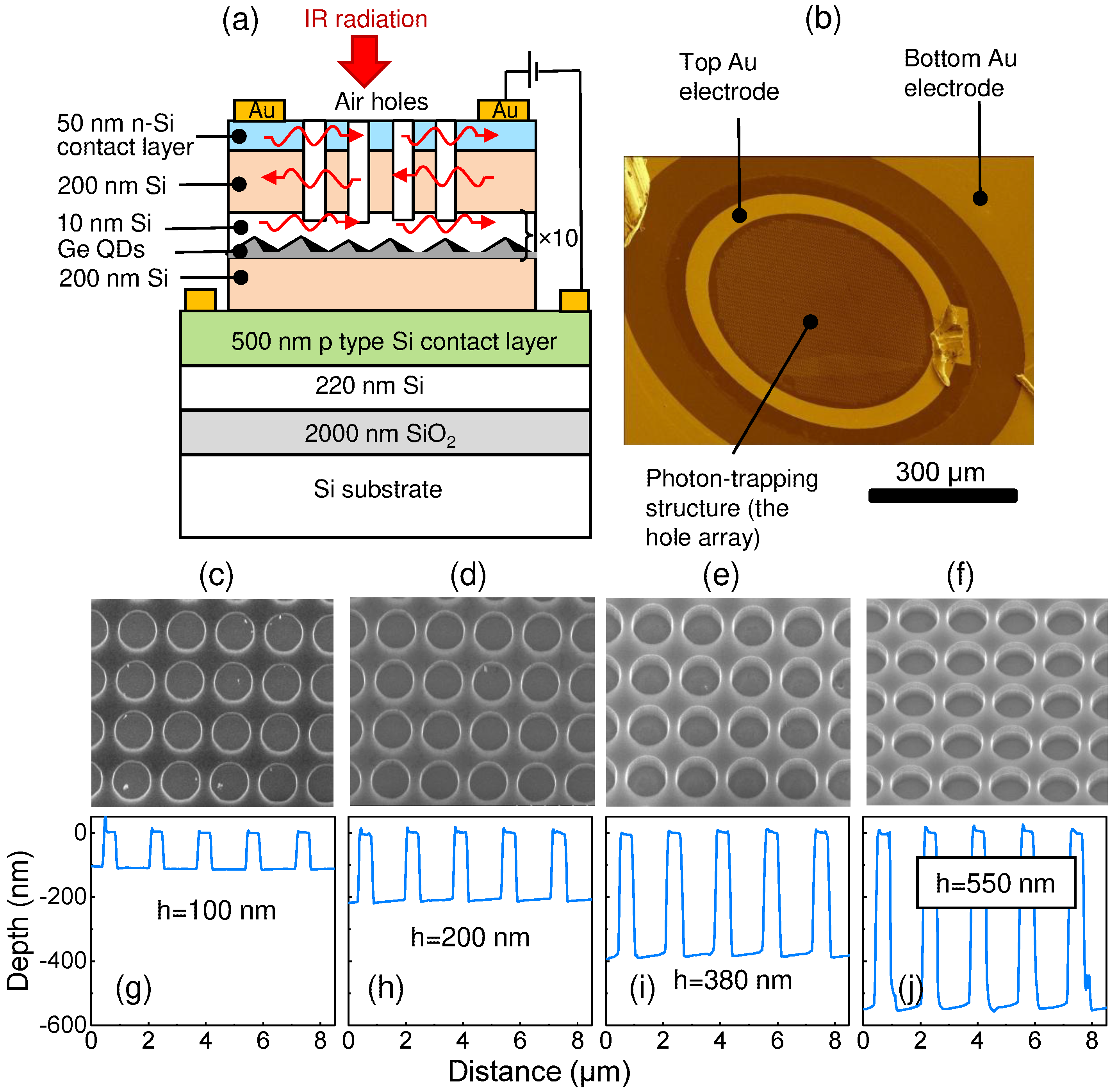
Abstract
:1. Introduction
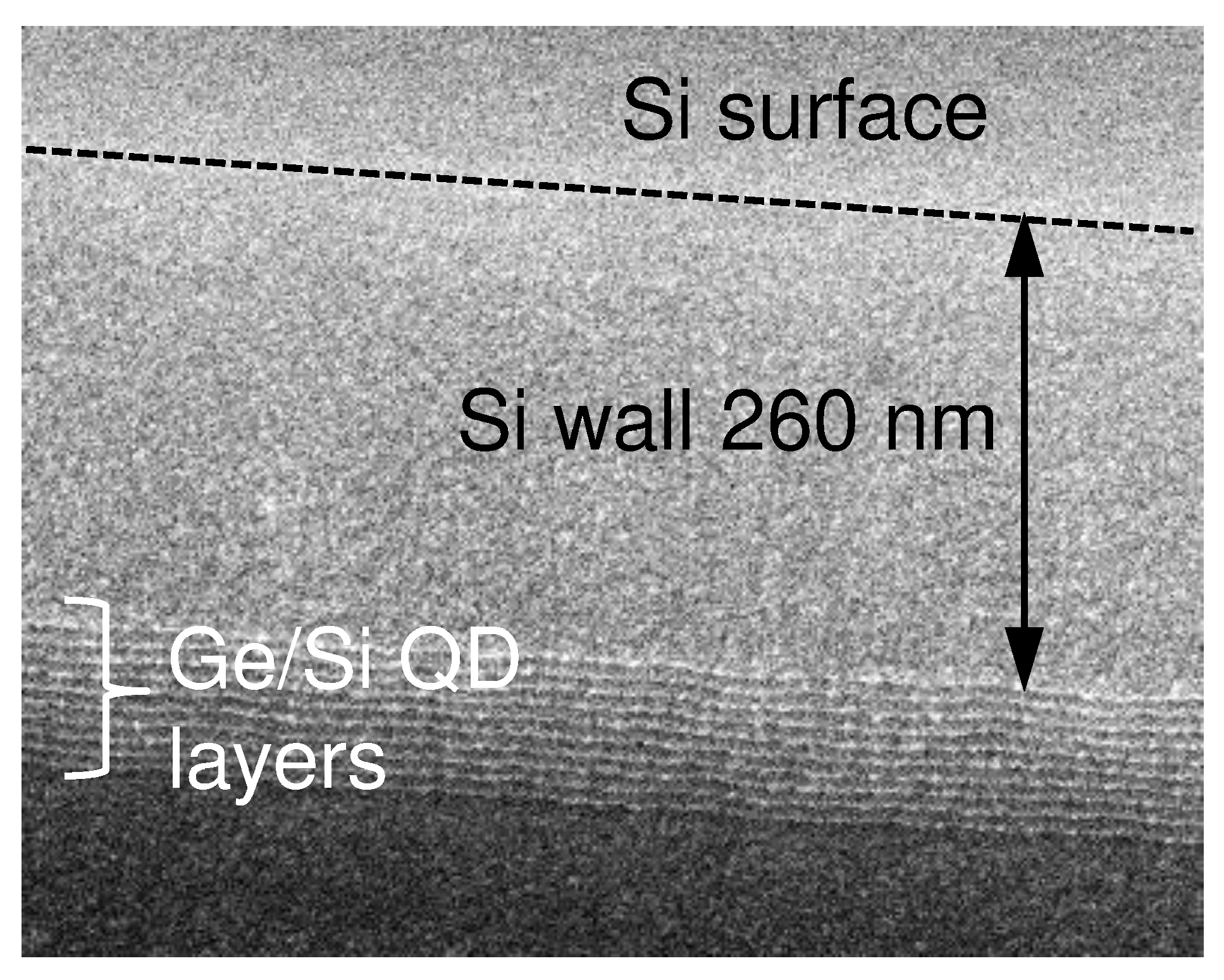
2. Materials and Methods
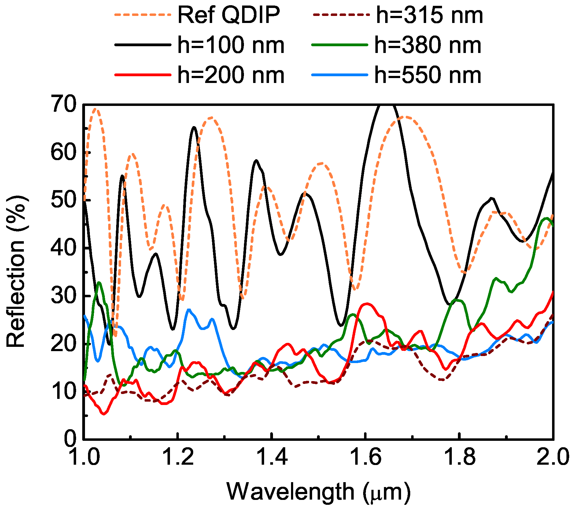
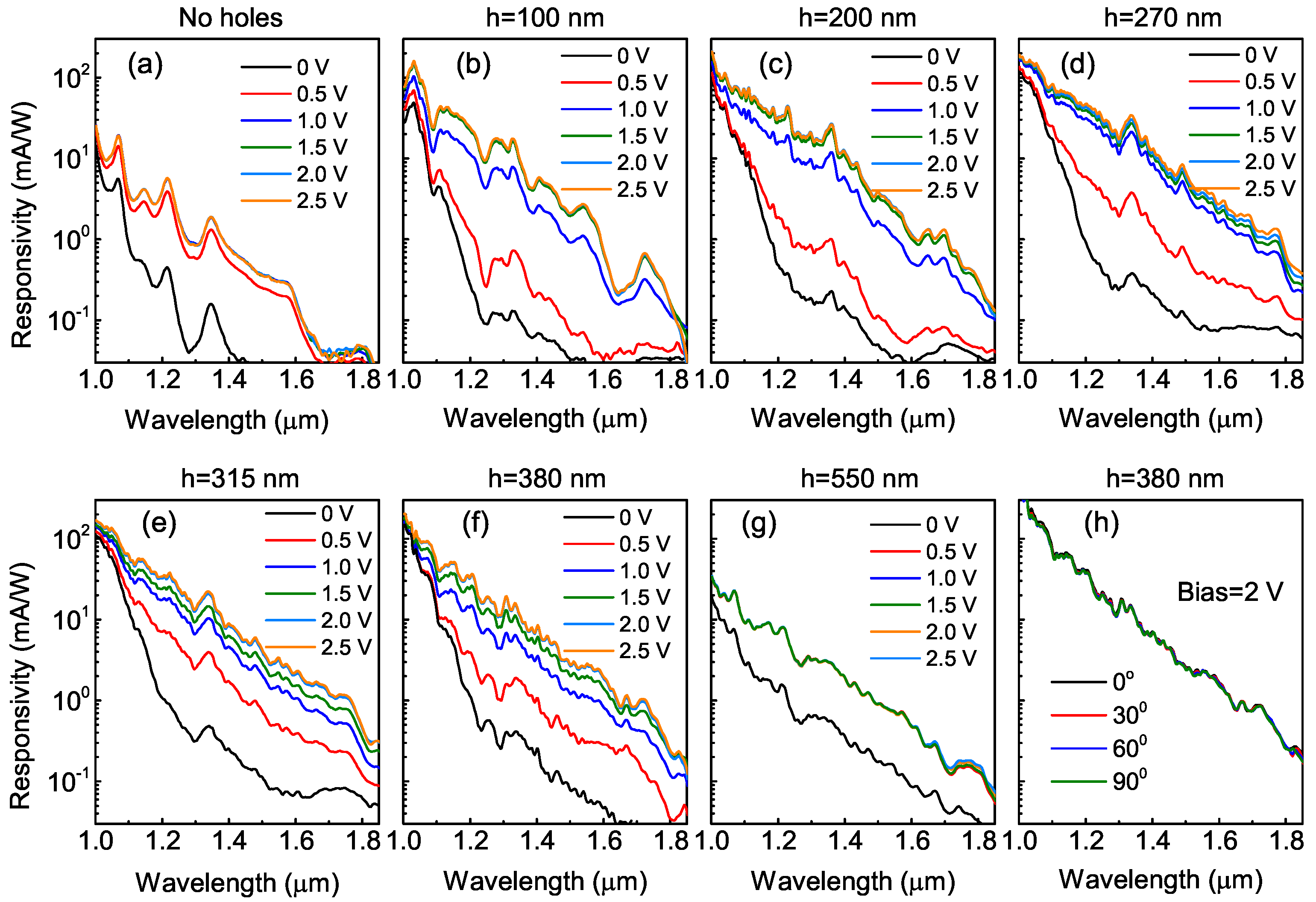
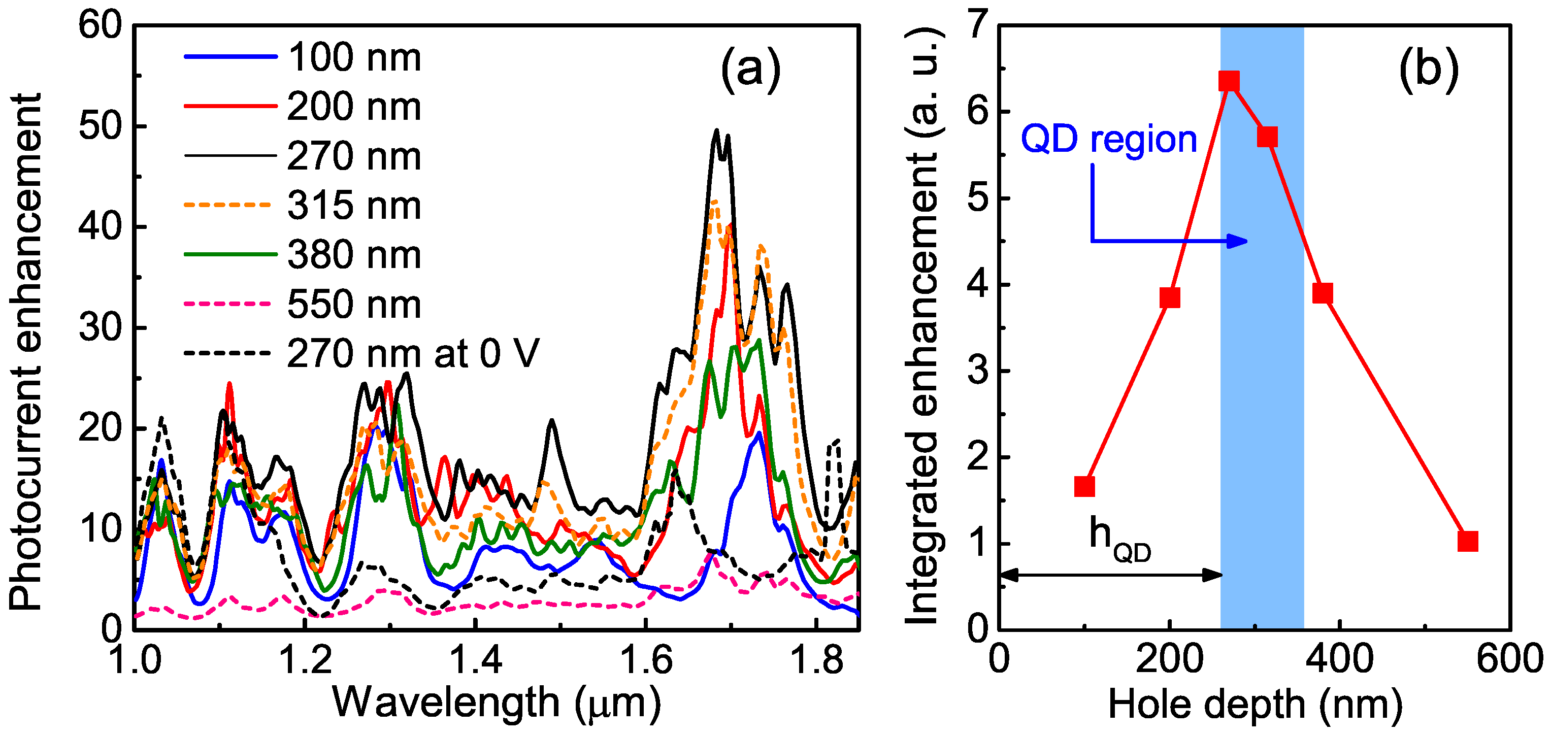
3. Results and Discussion
4. Conclusions
Author Contributions
Funding
Institutional Review Board Statement
Informed Consent Statement
Data Availability Statement
Acknowledgments
Conflicts of Interest
Abbreviations
| QD | Quantum dot |
| IR | Infrared |
| QDIP | Quantum dot infrared photodetector |
| MBE | Molecular beam epitaxy |
| SEM | Scanning electron microscopy |
| AFM | Atomic force microscopy |
| LED | Light-emitting diode |
References
- Tong, S.; Liu, J.; Wang, J.; Wang, K. Normal-incidence Ge quantum-dot photodetectors at 1.5 μm based on Si substrate. Appl. Phys. Lett. 2002, 80, 1189–1191. [Google Scholar] [CrossRef]
- Alguno, A.; Usami, N.; Ujihara, T.; Fujiwara, K.; Sazaki, G.; Nakajima, K.; Shiraki, Y. Enhanced quantum efficiency of solar cells with self-assembled Ge dots stacked in multilayer structure. Appl. Phys. Lett. 2003, 83, 1258–1260. [Google Scholar] [CrossRef]
- Elfving, A.; Hansson, G.; Ni, W.X. SiGe (Ge-dot) heterojunction phototransistors for efficient light detection at 1.3–1.55 μm. Physica E 2003, 16, 528–532. [Google Scholar] [CrossRef]
- Yakimov, A.I.; Kirienko, V.V.; Bloshkin, A.A.; Dvurechenskii, A.V.; Utkin, D.E. Near-infrared photoresponse in Ge/Si quantum dots enhanced by localized surface plasmons supported by aluminium nanodisks. J. Appl. Phys. 2020, 128, 143101. [Google Scholar] [CrossRef]
- Livache, C.; Martinez, B.; Goubet, N.; Gréboval, C.; Qu, J.; Chu, A.; Royer, S.; Ithurria, S.; Silly, M.G.; Dubertret, B.; et al. A colloidal quantum dot infrared photodetector and its use for intraband detection. Nat. Commun. 2019, 10, 2125. [Google Scholar] [CrossRef]
- Atwater, H.A.; Polman, A. Plasmonics for improved photovoltaic devices. Nat. Mater. 2010, 9, 205–213. [Google Scholar] [CrossRef] [PubMed]
- Tong, J.; Suo, F.; Ma, J.; Tobing, L.; Qian, L.; Zhang, D. Surface plasmon enhanced infrared photodetection. Opto-Electron. Adv. 2019, 2, 180026. [Google Scholar] [CrossRef]
- Wang, D.; Koh, Y.R.; Kudyshev, Z.A.; Maize, K.; Kildishev, A.V.; Boltasseva, A.; Shalaev, V.M.; Shakouri, A. Spatial and temporal nanoscale plasmonic heating quantified by thermoreflectance. Nano Lett. 2019, 19, 3796–3803. [Google Scholar] [CrossRef]
- Liu, H.; Kang, Y.; Meng, T.; Tian, C.; Wei, G. High photon absorptivity of quantum dot infrared photodetectors achieved by the surface plasmon effect of metal nanohole array. Nanoscale Res. Lett. 2020, 15, 98. [Google Scholar]
- Gao, Y.; Cansizoglu, H.; Polat, K.G.; Ghandiparsi, S.; Kaya, A.; Mamtaz, H.H.; Mayet, A.S.; Wang, Y.; Zhang, X.; Yamada, T.; et al. Photon-trapping microstructures enable high-speed high-efficiency silicon photodiodes. Nat. Photonics 2017, 11, 301–309. [Google Scholar] [CrossRef]
- Cansizoglu, H.; Bartolo-Perez, C.; Gao, Y.; Ponizovskaya Devine, E.; Ghandiparsi, S.; Polat, K.G.; Mamtaz, H.H.; Yamada, T.; Elrefaie, A.F.; Wang, S.Y.; et al. Surface-illuminated photon-trapping high-speed Ge-on-Si photodiodes with improved efficiency up to 1700 nm. Photonics Res. 2018, 6, 734–742. [Google Scholar]
- Cansizoglu, H.; Ponizovskaya Devine, E.; Gao, Y.; Ghandiparsi, S.; Yamada, T.; Elrefaie, A.F.; Wang, S.Y.; Islam, M.S. A new paradigm in high-speed and high-efficiency silicon photodiodes for communication – Part I: Enhancing photon-material interaction via low-dimensional structures. IEEE Trans. Electron Devices 2018, 65, 372–381. [Google Scholar] [CrossRef]
- Ghandiparsi, S.; Elrefaie, A.F.; Mayet, A.S.; Landolsi, T.; Bartolo-Perez, C.; Cansizoglu, H.; Gao, Y.; Mamtaz, H.H.; Golgir, H.R.; Ponizovskaya Devine, E.; et al. High-speed high-efficiency pin photodiodes for short-reach optical interconnects in data centers. IEEE J. Lightwave Tech. 2019, 37, 5748–5755. [Google Scholar] [CrossRef]
- Zhou, H.; Xu, S.; Lin, Y.; Huang, Y.C.; Son, B.; Chen, Q.; Guo, X.; Lee, K.H.; Gon, S.C.; Gong, X.; et al. High-efficiency GeSn/Ge multiple-quantum-well photodetectors with photon-trapping microstructures operating at 2 μm. Opt. Express 2020, 28, 10280–10293. [Google Scholar] [CrossRef]
- Suo, F.; Tong, J.; Chen, X.; Xu, Z.; Zhang, D.H. Hole array enhanced dual-band infrared photodetection. Opt. Express 2021, 29, 6424–6433. [Google Scholar]
- Suo, F.; Tong, J.; Zhang, D.H. Photon-trapping array for enhanced midwave infrared photoresponse. J. Phys. D Appl. Phys. 2021, 54, 505105. [Google Scholar]
- Zhou, H.; Chen, Q.; Wu, S.; Zhang, L.; Guo, X.; Son, B.; Tan, C.S. Grating and hole-array enhanced germanium lateral p-i-n photodetectors on an insulator platform. Opt. Express 2022, 30, 4706–4717. [Google Scholar] [CrossRef]
- Khurgin, J.B. Replacing noble metals with alternative materials in plasmonic and metamaterials: How good an idea? Phil. Trans. R. Soc. A 2017, 375, 20160068. [Google Scholar]
- Krasnok, A.E.; Miroshnichenko, A.E.; Belov, P.A.; Krishar, Y.S. All-dielectric optical nanoantennas. Opt. Express 2012, 20, 20599–20604. [Google Scholar] [CrossRef] [PubMed]
- Moitra, P.; Slovick, B.; Ya, Z.G.; Krishnamurthy, S. Experimental demonstration of a broadband all-dielectric metamaterial perfect reflector. Appl. Phys. Lett. 2014, 104, 171102. [Google Scholar]
- Jahani, S.; Jacob, Z. All-dielectric metamaterials. Nat. Nanotechnol. 2016, 11, 23–36. [Google Scholar] [CrossRef] [PubMed]
- Decker, M.; Staude, I. Resonant dielectric nanostructures: A low-loss platform for fucntional nanophotonics. J. Opt. 2016, 18, 103001. [Google Scholar] [CrossRef]
- Kamali, S.M.; Arbabi, E.; Arbabi, A.; Faraon, A. A review of dielectric optical metasurfaces for wavefront control. Nanophotonics 2018, 7, 1041–1068. [Google Scholar] [CrossRef]
- Liu, M.; Fan, Q.; Yu, L.; Xu, T. Polarization-independent infrared micro-lens array based on all-silicon metasurfaces. Opt. Express 2019, 27, 10738–10744. [Google Scholar] [CrossRef]
- Yakimov, A.I.; Kirienko, V.V.; Bloshkin, A.A.; Utkin, D.E.; Dvurechenskii, A.V. Near-infrared photoresponse in Ge/Si quantum dots enhanced by photon-trapping hole arrays. Nanomaterials 2021, 11, 2302. [Google Scholar] [CrossRef]
- Yakimov, A.I.; Nikiforov, A.I.; Dvurechenskii, A.V.; Ulyanov, V.V.; Volodin, V.A.; Groetzschel, R. Effect of growth rate on the morphology and structural properties of hut-shaped Ge islands in Si(001). Nanotechnology 2006, 17, 4743–4747. [Google Scholar] [CrossRef] [PubMed] [Green Version]
- Yakimov, A.I.; Kirienko, V.V.; Armbrister, V.A.; Bloshkin, A.A.; Dvurechenskii, A.V. Photoconductive gain and quantum efficiency of remotely doped Ge/Si quantum dot photodetectors. Mater. Res. Express 2016, 3, 105032. [Google Scholar]
- Zang, K.; Jiang, X.; Huo, Y.; Ding, X.; Morea, M.; Chen, X.; Lu, C.Y.; Ma, J.; Zhou, M.; Xia, Z.; et al. Silicon single-photon avalanche diodes with nanostructured light trapping. Nat. Commun. 2017, 8, 628. [Google Scholar] [CrossRef]
- Tong, J.; Tobing, L.; Zhang, D. Electrically controlled enhancement in plasmonic mid-infrared photodiode. Opt. Express 2018, 26, 5452–5460. [Google Scholar] [CrossRef]
- Yamada, T.; Ponizovskaya Devine, E.; Ghandiparsi, S.; Bartolo-Perez, C.; Mayet, A.S.; Cansizoglu, H.; Gao, Y.; Ahamed, A.; Wang, S.Y.; Islam, M.S. Modeling of nanohole silicon pin/nip photodetectors: Steady state and transient characteristics. Nanotechnology 2021, 32, 365201. [Google Scholar]
- Baba, T. Slow light in photonic crystals. Nat. Photonics 2008, 2, 465–473. [Google Scholar] [CrossRef]
- Duché, D.; Escoubas, L.; Simon, J.J.; Torchio, P.; Vervisch, W.; Flory, F. Slow Bloch modes for enhancing the absorption of light in thin films for photovoltaic cells. Appl. Phys. Lett. 2008, 92, 193310. [Google Scholar] [CrossRef]


Publisher’s Note: MDPI stays neutral with regard to jurisdictional claims in published maps and institutional affiliations. |
© 2022 by the authors. Licensee MDPI, Basel, Switzerland. This article is an open access article distributed under the terms and conditions of the Creative Commons Attribution (CC BY) license (https://creativecommons.org/licenses/by/4.0/).
Share and Cite
Yakimov, A.I.; Kirienko, V.V.; Utkin, D.E.; Dvurechenskii, A.V. Light-Trapping-Enhanced Photodetection in Ge/Si Quantum Dot Photodiodes Containing Microhole Arrays with Different Hole Depths. Nanomaterials 2022, 12, 2993. https://doi.org/10.3390/nano12172993
Yakimov AI, Kirienko VV, Utkin DE, Dvurechenskii AV. Light-Trapping-Enhanced Photodetection in Ge/Si Quantum Dot Photodiodes Containing Microhole Arrays with Different Hole Depths. Nanomaterials. 2022; 12(17):2993. https://doi.org/10.3390/nano12172993
Chicago/Turabian StyleYakimov, Andrew I., Victor V. Kirienko, Dmitrii E. Utkin, and Anatoly V. Dvurechenskii. 2022. "Light-Trapping-Enhanced Photodetection in Ge/Si Quantum Dot Photodiodes Containing Microhole Arrays with Different Hole Depths" Nanomaterials 12, no. 17: 2993. https://doi.org/10.3390/nano12172993